- Product Description Description
- Table of Contents TOC
- List of Table & Figure LOT
- Get Free Sample PDF Sample PDF
Market Size, 2025
$923.5 MnMarket Estimate, 2026
$995.1 MnMarket Forecast, 2034
$1808 MnCAGR, 2026–2034
7.75%Europe Chemical Mechanical Planarization Market Report Summary
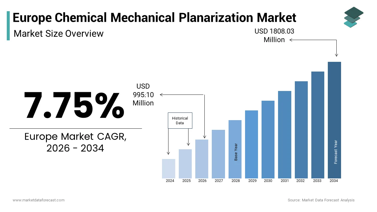
The Europe chemical mechanical planarization (CMP) market was valued at USD 923.53 million in 2025, is estimated to reach USD 995.10 million in 2026, and is projected to expand to USD 1808.03 million by 2034, growing at a CAGR of 7.75% during the forecast period from 2026 to 2034. The market’s growth is driven by the rapid expansion of semiconductor manufacturing in Europe, rising demand for advanced integrated circuits, and increasing investments in automotive electronics, compound semiconductors, and next-generation chip technologies.
The Europe CMP market benefits from the region’s strategic push to strengthen domestic semiconductor supply chains, reduce reliance on imports, and support innovation in advanced packaging and “More Than Moore” technologies. Increasing adoption of CMP processes for ultra-flat wafer surfaces in logic, memory, and power devices is further accelerating market growth.
Key Market Trends
- Rising adoption of More Than Moore technologies for heterogeneous integration and advanced packaging.
- Strong demand for CMP consumables due to their recurring replacement cycles and process-critical role.
- Increasing use of CMP in automotive electronics, compound semiconductors, and power devices.
- Continuous innovation in slurry formulations to improve yield, selectivity, and defect control.
- Growing emphasis on localized semiconductor manufacturing is supported by European industrial policies.
Segmental Insights
- Based on type, the CMP consumables segment dominated the Europe chemical mechanical planarization market in 2024. This dominance is attributed to the high consumption rate of slurries, pads, and conditioners required across multiple wafer processing steps.
- Based on technology, the More Than Moore segment held 58.3% of the market share in 2024. Its leadership is driven by Europe’s strong focus on compound semiconductors, sensors, power electronics, and heterogeneous integration rather than pure logic scaling.
- Based on application, the integrated circuits segment accounted for 45.3% of the Europe CMP market share in 2024, supported by increasing IC complexity, miniaturization, and demand from automotive, industrial, and communication applications.
Country-Level Insights
- Germany emerged as the largest market, capturing 26.3% of the Europe CMP market share in 2024, driven by its strong automotive electronics base, industrial semiconductor demand, and advanced manufacturing ecosystem.
- France ranked second with a 19.3% share, supported by robust semiconductor R&D and fabrication activities.
- The Netherlands is poised for steady growth due to its position as a global hub for semiconductor equipment and materials.
- Italy is witnessing growth led by large-scale compound semiconductor operations, particularly in Sicily.
- The United Kingdom market is expanding through developments in compound semiconductors and quantum technologies rather than high-volume chip production.
Competitive Landscape
The Europe chemical mechanical planarization market is moderately consolidated, with global and regional players focusing on innovation, customized CMP solutions, and long-term partnerships with semiconductor manufacturers. Key companies operating in the market include Air Products & Chemicals, Inc., Applied Materials, Inc., BASF SE, Dow Electronic Materials, DuPont Electronic Solutions, Ebara Corporation, Fujimi Incorporated, Hitachi Chemical Company, Ltd., Lapmaster Wolters GmbH, LAM Research Corporation, Cabot Microelectronics Corporation, Okamoto Machine Tool Works, Ltd., Sungmoon Electronics Co., Ltd., and Strasbaugh In.
Europe Chemical Mechanical Planarization Market Size
The Europe chemicals mechanical planarization market size was valued at USD 923.53 million in 2025 and is anticipated to reach a valuation of USD 995.10 million in 2026 and USD 1808.03 million by 2034, growing at a CAGR of 7.75% from 2026 to 2034.
Current Introduction of the Europe Chemical Mechanical Planarization Market
The chemical mechanical planarization is the regional ecosystem supplying specialized slurries, pads, and equipment used to achieve nanoscale surface flatness during semiconductor and advanced packaging fabrication. Europe’s relevance in this domain stems not from mass chip production but from industrial automation, automotive electronics,s and compound semiconductor innovation, sectors demanding high-reliability microelectronics. Furthermore, as per the European Commission, Europe’s semiconductor fabs specialize in mature and specialized nodes below 28 nanometers, where planarization remains indispensable for yield optimization. The region’s adherence to stringent chemical handling regulations under REACH and the Industrial Emissions Directive also shapes formulation design, favoring low toxicity, biodegradable slurry components.
MARKET DRIVERS
Expansion of Advanced Packaging for Automotive and Industrial Electronics
The accelerating adoption of advanced packaging technologies, such as fan-out wafer-level packaging and 2.5D integration in automotive and industrial applications, is a primary driving factor for the growth of Europe's chemical mechanical planarization market. Modern electric vehiclesnow integrate over 3000 semiconductor devices per unit, according to the European Automobile Manufacturers Association, many requiring redistribution layers and through silicon vias that necessitate multiple planarization steps. Infineon and STMicroelectronics Europe’s leading chipmakers have expanded their Dresden and Agrate Brianza fabs to produce silicon carbide power modules, where planarization ensures defect-free metal interconnects under high thermal stress. As per the European Power Electronics and Applications Association, many new automotive power modules produced in Europe in 2024 employed at least 2 chemical mechanical planarization cycles during backend processing. Additionally, the European Union’s Chips Act has allocated 3.6 billion euros to bolster domestic advanced packaging capacity with pilot lines at imec Sweden and CEA Leti France, prioritizing planarization process integration. This strategic focus on high-value specialized semiconductors rather than logic scaling sustains robust and technically demanding consumption of planarization consumables across the region.
Rising Investment in Compound Semiconductor Manufacturing
Europe’s strategic pivot toward compound semiconductors, particularly gallium nitride and silicon carbide, de for 5G infrastructure and renewable energy systems is intensifying chemical mechanical planarization utilization. The rising investment in compound semiconductor manufacturing is also gearing up for the growth of Europe chemical mechanical planarization market. These materials exhibit extreme hardness and chemical inertness, requiring specialized slurries with tailored abrasive particles and pH stabilizers. According to the European Institute of Innovation and Technology, over 12 new compound semiconductor pilot lines became operational across Germany, France, and the Netherlands between 2022 and 2024. The UK’s Compound Semiconductor Centre in Wales reported that gallium nitride wafer processing now includes three to four planarization steps per device to achieve surface roughness below 0.5 nanometers for radio frequency performance. Moreover, the designated wide bandgap semiconductors, as a strategic technology with 800 million euros committed to domestic supply chain development through 2027, as pethe r the source. This institutional backing ensures sustained investment in fabrication infrastructure where planarization is non-substitutable for defect control. Consequently, the unique material properties and performance requirements of compound semiconductors create a high barrier, high precision niche that anchors chemical mechanical planarization as an essential process in Europe’s semiconductor sovereignty agenda.
MARKET RESTRAINTS
Stringent Environmental and Chemical Handling Regulations
The region’s rigorous regulatory framework governing chemical use and waste disposal in microelectronics manufacturing is one of the restraints for the growth ofEurope'se chemical mechanical polarization market. The EU’s REACH regulation classifies many conventional slurry components, such as certain cerium oxide dispersions and organic additives, as substances of very high concern requiring extensive authorization. As per the European Chemicals Agency, over 40% of slurry formulations used globally are either restricted or require site-specific permits for use in EU fabs. Compliance necessitates reformulation with biodegradable chelating agents and low metal content abrasives, which often compromise removal rate or surface quality. Additionally, the Industrial Emissions Directive mandatesclosed-loopp slurry recycling systems with less than 5% discharge tolerance, audit of semiconductor facilities. These systems cost between 1.5 and 2.5 million euros per installation, according to VDM,, A the German engineering association, increasing operational overhead for smaller fabs. The cumulative effect is delayed process qualification, longer validation cycles, and a higher total cost of ownership that disproportionately impact European fabs competing against less-regulated global counterparts.
Limited Domestic Semiconductor Fabrication Scale
The relatively modest volume of front-end wafer fabrication compared to Asia and North America constrains the scale economics of chemical mechanical planarization consumption. This factor is also declining the growth of Europe chemical mechanical planarization market. This limited throughput reduces purchasing leverage for slurry and pad suppliers, who prioritize high-volume regions for new formulation launches. As a result, European fabs often receive second-tier technical support or delayed access to next-generation consumables optimized for advanced nodes. Furthermore, European fabs operate below 70% capacity utilization due to fragmented demand across the automotive, industrial, and aerospace sectors. This underutilization discourages suppliers from establishing localized formulation or conditioning service,s, increasing lead times and inventory costs.
MARKET OPPORTUNITIES
Development of Eco-Friendly and High-Precision Slurry Formulations
The next generation planarization slurries that reconcile environmental compliance with nanoscale performance are creating new opportunities for the growth of Europe chemical mechanical planarization market. Driven by EU Green Deal mandates and corporate sustainability ttargetss semiconductor chemical suppliers are investing in bio-based dispersants and recyclable abrasive systems. As per the Fraunhofer Institute, researchers in Germany have engineered silica-based slurries with zwitterionic surfactants that achieve 99.8% biodegradability, while maintaining removal rates above 300 nanometers per minute on copper layers. Companies like BASF and Solvay have partnered with CEA Leti to co-develop low chemical oxygen demand slurries that reduce wastewater treatment costs, as verified in 2024 pilot trials at STMicroelectronics’ Rousset facility. Additionally, the European Partnership for Key Digital Technologies called PLANAR ECO to establish a circular slurry supply chain with on-site regeneration units. This innovation ecosystem transforms regulatory pressure into competitive advantage, enabling European suppliers to export compliant high-performance formulations to environmentally conscious fabs globally.
Integration of In-Line Metrology and AI-Driven Process Control
The emergence of real-time metrology and artificial intelligence in planarization process optimization presents a high-value opportunity for Europe’s equipment and materials ecosystem. The integration of in-line metrology and AI-driven process control is additionally leveraging the growth of Europe chemical mechanical planarization market. European semiconductor toolmakers, such as SPTS Technologies and EV Group, are embedding interferometric sensors and acoustic emission monitors directly into planarization platforms to enable endpoint detection without wafer removal. According to the European Association of Automotive Suppliers, integration of these systems reduced over-polishing defects by 33% in power module production during 2024 trials at Bosch’s Reutlingen fab. Furthermore, the EU Horizon Europe program has supported the AICMP project, which uses machine learning to correlate slurry chemistry, wear pad topography, nd removal rate in real time, lowering dynamic slurry dosing adjustments.
MARKET CHALLENGES
High Cost and Complexity of Slurry Customization for Diverse Substrates
The escalating complexity of slurry formulation required to address the region’s heterogeneous substrate is one of the challenges for the growth of Europe chemical mechanical planarization market. Unlike high-volume memory or logic fabs that process uniform materials, European facilities handle silicon carbide, gallium nitride, and silicon on insulator or copper interconnects within the same cleanroom, necessitating frequent slurry changeovers. As per VTT Technical Research Centre of Finland, each new material combination requires at least 12 weeks of slurry qualification involving over 200 test wafers to validate defect density and dishing control. This customization burden is compounded by limited access to proprietary slurry additives as major global suppliers restrict formulation data under intellectual property agreements. Consequently, European fabs often resort to in-house blending, which increases contamination risk and process variability. This operational fragility undermines throughput and escalates the cost of ownership in an already capital-intensive environment.
Shortage of Skilled Technicians for Advanced Planarization Processes
Europe faces a growing deficit of process engineers and technicians trained in the intricacies ofadvanced nodes and compound semiconductors is additionally hhamperssthe growth of Europe's chemical mechanical planarization market. According to the European Skills Agenda, the semiconductor manufacturing unfilled vacancy rate for process integration roles in 2024, with planarization cited as one of the most specialized competencies. The complexity arises from the need to balance chemical kikineticss mechanical abrasion, and thermal effects simultaneously with a skill set rarely covered in standard engineering curricula. This gap forces fabs to rely on vendor-supported training, which is often generic and not tailored to local material stacks.
REPORT COVERAGE
| REPORT METRIC | DETAILS |
| Market Size Available | 2025 to 2034 |
| Base Year | 2025 |
| Forecast Period | 2026 to 2034 |
| CAGR | 7.75% |
| Segments Covered | By Type, Technology, Application, and By Country |
| Various Analyses Covered | Global, Regional & Country Level Analysis, Segment-Level Analysis, DROC, PESTLE Analysis, Porter’s Five Forces Analysis, Competitive Landscape, Analyst Overview on Investment Opportunities |
| Regions Covered | UK, France, Spain, Germany, Italy, Russia, Sweden, Denmark, Switzerland, Netherlands, Turkey, the Czech Republic, and the Rest of Europe |
| Market Leaders Profiled | Air Products & Chemicals, Inc., Applied Materials, Inc., BASF SE, DOW Electronic Materials, DuPont Electronic Solutions, Ebara Corporation, Fujimi Incorporated, Hitachi Chemical Company, Ltd., Lapmaster Wolters GmbH, LAM Research Corporation, Cabot Microelectronics Corporation, Okamoto Machine Tool Works, Ltd., Sungmoon Electronics Co., Ltd., Strasbaugh Inc. |
SEGMENTAL ANALYSIS
By Type Insights
The CMP consumables segment was the largest by holding a dominant share of the Europe chemical mechanical planarization market in 2025, due to their recurring usage pattern and high replacement frequency compared to capital-intensive equipment. Every planarization cycle consumes slurry and gradually wears down pads, necessitating replenishment every 500 to 1500 wafer passes. The European Semiconductor Equipment Industry Consortium confirmed that consumables represent total planarization operational expenditure due to strict purity requirements and material compatibility constraints. Additionally, EU REACH regulations have accelerated the shift toward customized low-toxicity slurry formulations, which command premium pricing and require frequent reformulation as new materials like silicon carbide enter production. This combination of process intensity, y regulatory complexity,y, and consumable turnover ensures that materials,n ot machines, anchor the market’s economic gravity.
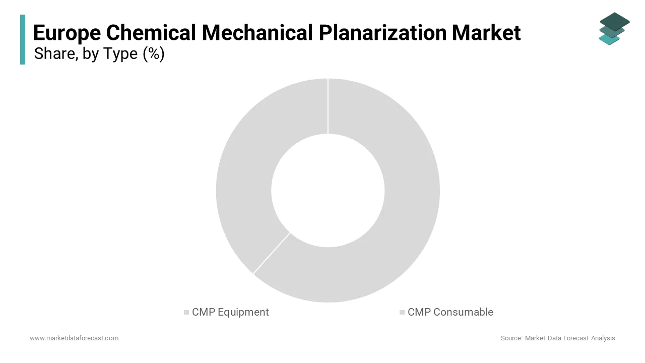
The CMP consumables segment is lucratively growing with an expected CAGR of 7.9% throughout the forecast period, owing to Europe’s strategic focus on compound semiconductors and advanced packaging, where planarization intensity per device has increased significantly. As per the European Power Electronics and Applications Association, each silicon carbide power module now requires 3 to 4 planarization steps, double the count for traditional silico, due to its extreme hardness and surface defect sensitivity. The Fraunhofer Institute reported in 2025 that slurry consumption per wafer in gallium nitride RF device fabrication rose, when compared to 2021, owing totighter surface roughness tolerances below 0.3 nanometers. Unlike equipment, which is purchased once per fab expansion, consumables scale directly with wafer output by making them the most responsive barometer of Europe’s semiconductor manufacturing resurgence.
By Technology Insights
The More Than Moore’s technology segment accounted in holding 58.3% of the Europe chemical mechanical planarization market share in 2025, with the region’s specialization in application-specific semiconductors rather than logic scaling. This category encompasses power electronics, MEMS sensors, and analog chips used in automotive, industrial, and medical devices sectors. According to the European Semiconductor Industry Association, European wafer starts in 2025 were dedicated to More Than Moore’s technologies, primarily for electric vehicle inverters and industrial automation controllers. These devices often integrate multiple materials, including copper, aluminum, and silicon carbide r, requiring repeated planarization to manage topography across heterogeneous layers. The European Automobile Manufacturers Association noted that a single electric vehicle platform now incorporates up to nine distinct planarized power modules, each demanding a high precision surface finish to ensure bond reliability. This material complexity and application criticality make planarization indispensable in Europe’s semiconductor value chain, which prioritizes functional integration over transistor density.
The quantum computin otonics, neuromorphic chips and 3D heterogeneous integration segment is projected to grow at a CAGR of 9.3% from 2026 to 2034 with Europe’s heavy investment in next-generation computing infrastructure and sovereign tech capabilities. As per the European Innovation Council, over 14 quantum and photonic pilot lines became operational across Europe between 2022 and 2024, including the Quantum Delta NL initiative in the Netherlands and the Quantum Computing Initiative in Germany. These advanced platforms require atomically flat surfaces on non-traditional substrates such as lithium niobate and indium phosphide, where conventional slurries fail. The CEA Leti institute in France reported that photonic integrated circuits demand surface roughness below 0.1 nanometers, a chievable only through multi-stage planarization with customized ceria-based slurries. This convergence of public funding s, scientific ambition, and ultra-precision requirements positions emerging technologies as the high-growth frontier of Europe’s planarization market.
By Application Insights
The integrated circuits segment was the largest by occupying 45.3% of the Europe chemical mechanical planarization market share in 2025 due to their foundational role in automotive microcontrollers, power management IICs,s and industrial processors. Although Europe does not mass-produce leading-edge logic chips, it maintains robust production of specialized ICs below 28 nnanometers where planarization ensures metal interconnect integrity and via reliability. According to SEMI Europe, over 12 billion integrated circuit units were fabricated in European fabs in 2025, destined for automotive applications. Each of these devices typically undergoes 6 to 10 planarization steps during backend processing to flatten copper and dielectric layers. Furthermore, the European Chips Act’s emphasis on secure and reliable domestic IC supply chains has triggered fab upgrades that increase planarization tool utilization and consumable throughput, enforcing this segment’s dominance.
The compound semiconductors segment is lucratively growing with an expected CAGR of 10.1% throughout the forecast period, with Europe’s strategic commitment to energy efficiency and 5G infrastructure, which rely on gallium nitride and silicon carbide devices. These materials pose extreme planarization challenges due to their high hardness and chemical stability, requiring specialized slurries with diamond or ceria abrasives and extended polishing times. The UK’s Compound Semiconductor Applications Catapult verified that each gallium nitride RF wafer now undergoes 4 planarization steps compared to 2 for silicon, effectively doubling consumable use per unit. This confluence of performance, necessity, industrial policy nd material complexity drives disproportionate growth in this high-value application.
COUNTRY LEVEL ANALYSIS
Germany Chemical Mechanical Planarization Market Analysis
Germany was the top performer of the Europe chemical mechanical planarization market by capturing 26.3% of the market share in 2025, driven by its world-leading automotive and industrial electronics manufacturing base. The country hosts major semiconductor fabs, including Infineon’s 300 millimeter facility in Dresden and Bosch’s advanced MEMS plant in Reutlingen, both of which rely heavily on planarization for power electronics and sensor production. The Fraunhofer Institute in Dresden reported that planarization process development for silicon carbide in Europe occurs within German research clusters. Additionally, Germany’s engineering ecosystem, including equipment makers like SPTS and chemical suppliers like BASF, creates a vertically integrated innovation loop that accelerates process adoption.
France Chemical Mechanical Planarization Market Analysis
The French chemical mechanical planarization market held second position by holding 19.3% of the market share in 2025, with its strong research infrastructure and strategic investments in secure electronics. The country’s CEA Leti institute in Grenoble is a global hub for advanced packaging and emerging technology development, where planarization is integral to 3D integration and photonic chip fabrication. The French Ministry of Armed Forces confirmed that many other domestic defense electronics now require compound semiconductor planarization for radar and communication systems. Furthermore, France’s dominance in quantum computing through the Quantum Plan has established 6 new pilot lines that demand atomic-level surface control.
Netherlands Chemical Mechanical Planarization Market Analysis
The Netherlands chemical mechanical planarization market growth is likely to grow with its position as a global semiconductor equipment and materials hub. While domestic wafer production is modest, the presence of ASMLAEC, and NXP creates a dense ecosystem of process development and supplier collaboration. According to the Netherlands Foreign Investment Agency, many of the global semiconductor equipment suppliers maintain R and D centers in the Dutch Brainport region, where planarization integration is tested alongside lithography and etch modules. Additionally, the Dutch Ministry of Economic Affairs reported that semiconductor-related exports grew in 2024, with consumables and process services contributing significantly.
Italy Chemical Mechanical Planarization Market Analysis
Italy's chemical mechanical planarization market growth is likely to be driven by STMicroelectronics’ massive compound semiconductor operations in Catania, Sicily. This facility is Europe’s largest silicon carbide wafer fab,p producingover 40000 six-inch equivalent wafers per month as per the Italian Ministry of Enterprise and Made in Italy. The University of Bologna also launched Europe’s first master’s program in semiconductor planarization science in 2025, addressing workforce gaps. Italy’s market strength thus lies in its focused vertical integration around wide bandgap semiconductors.
United Kingdom Chemical Mechanical Planarization Market Analysis
The United Kingdom chemical mechanical planarization market growth is likely to grow with the compound semiconductors and quantum technologies, rather than volume production. The Compound Semiconductor Applications Catapult in South Wales coordinates over 120 industry projects annually, where planarization is for gallium nitride RF devices used in 5G base stations. According to Innovate UK, government funding for semiconductor materials processing exceeded 200 million pounds in 2025, with planarization identified as a key factor in yield improvement. The National Quantum Computing Centre in Harwell requires atomically flat substrates for superconducting qubits, necessitating custom ceria slurry formulations developed in partnership with Oxford University. Additionally, UK fabs such as IQE have adopted in-house slurry regeneration systems to comply with strict environmental permits from the Environment Agency.
COMPETITIVE LANDSCAPE
Competition in the Europe chemical mechanical planarization market is defined by technological specialization rather than volume scale, with participants focusing on high precision applications in automotive, e-power electronics, MEMS, and compound semiconductors. Global equipment leaders compete alongside European chemical and materials innovators, creating a hybrid ecosystem where integration and customization outweigh price considerations. Differentiation is achieved through regulatory cocompliance materialsciencee expert se and and, and digital process control rather than standard product offerings. The limited number of European fabs heightens the importance of long-term technical partnerships and co-development agreements. Barriers to entry remain high due to stringent purity standards, REACH compliance, and theneed forr on-siteapplicationn support.
KEY MARKET PLAYERS
A few of the market players in the Europe chemical mechanical planarization market are
- Air Products & Chemicals, Inc
- Applied Materials, Inc.
- Entegris Inc
- BASF SE
- DOW Electronic Materials
- DuPont Electronic Solutions
- Ebara Corporation
- Fujimi Incorporated
- Hitachi Chemical Company, Ltd
- Lapmaster Wolters GmbH
- LAM Research Corporation
- Cabot Microelectronics Corporation
- Okamoto Machine Tool Works, Ltd
- Sungmoon Electronics Co., Ltd.
- Strasbaugh Inc.
Top Players In The Market
- Applied Materials maintains a strategic presence in the Europe chemical mechanical planarization market through its advanced Reflexion and Mirra platform deployments across automotive and compound semiconductor fabs. The company supplies integrated planarization systems tailored for silicon carbide and gallium nitride processing, which are critical for European power electronics manufacturing. Applied Materials expanded its application development lab in Dresden, Germany, to support local customers wwith material-specificslurry and pad optimization. The company also launched its SmartFactory planarization analytics suite, enabling real-time endpoint detection and consumable forecasting. These initiatives reinforce Applied Materials’ role as a technology enabler in Europe’s specialized semiconductor ecosystem while aligning with the EU Chips Act’s goals for process sovereignty.
- BASF SE is a key contributor to the Europe chemical mechanical planarization market through its Performance Chemicals division,n which develophigh-purityty slurries and post CMP cleaning formulations. The company leverages its materials science expertise to create low-toxicity ceria and silica-based dispersions compliant with EU REACH regulations. BASF partnered with CEA Leti in France to co-develop biodegradable chelating agents for copper planarization that reduce wastewater treatment costs by over 35%. Additionally, BASF established a dedicated slurry formulation center in Ludwigshafen, Germany, focused on compound semiconductor applications. These actions position BASF as a sustainability-driven innovator supporting Europe’s transition toward environmentally responsible advanced manufacturing.
- Entegris plays a vital role in the Europe chemical mechanical planarization market by supplying high-purity filtration membranes, slurry delivery systems, ms and advanced pad conditioners. The company’s focus on contamination control aligns with European fabs’ stringent defect reduction targets, especially for power devices and MEMS. Entegris inaugurated a new European Technology Center in Berlin featuring a cleanroom dedicated to slurry compatibility testing and pad wear analysis. It also introduced its i2S intelligent slurry management platform, which monitors particle agglomeration in real time to prevent micro scratching.
Top Strategies Used by the Key Market Participants
Key players in the Europe chemical mechanical planarization market prioritize co-development of eco-friendly slurry formulations compliant with EU chemical regulations. They establish localized application labs near major fabs to accelerate process qualification for compound semiconductors and advanced packaging. Companies integrate digital analytics and real-time metrology into planarization platforms to enable predictive maintenance and endpoint accuracy. Strategic partnerships with research institutes such as CEA Leti and Fraunhofer support innovation in emerging materials like gallium nitride and silicon carbide. Additionally, they invest in circular economy initiatives, including slurry regeneration and pad recycling to align with Europe’s industrial sustainability mandates.
MARKET SEGMENTATION
This research report on the Europe chemical mechanical planarization market is segmented and sub-segmented into the following categories.
By Type
- CMP Equipment
- CMP Consumable
By Technology
- Leading Edge
- More Than Moore’s
- Emerging
By Application
- Integrated Circuits
- Mems And Nems
- Compound Semiconductors
- Optics
By Country
- UK
- France
- Spain
- Germany
- Italy
- Russia
- Sweden
- Denmark
- Switzerland
- Netherlands
- Turkey
- Czech Republic
- Rest of Europe