- Product Description Description
- Table of Contents TOC
- List of Table & Figure LOT
- Get Free Sample PDF Sample PDF
Market Size, 2025
$1.70 BnMarket Estimate, 2026
$1.85 BnMarket Forecast, 2034
$3.63 BnCAGR, 2026–2034
8.78%Europe Scanning Electron Microscope Market Report Summary
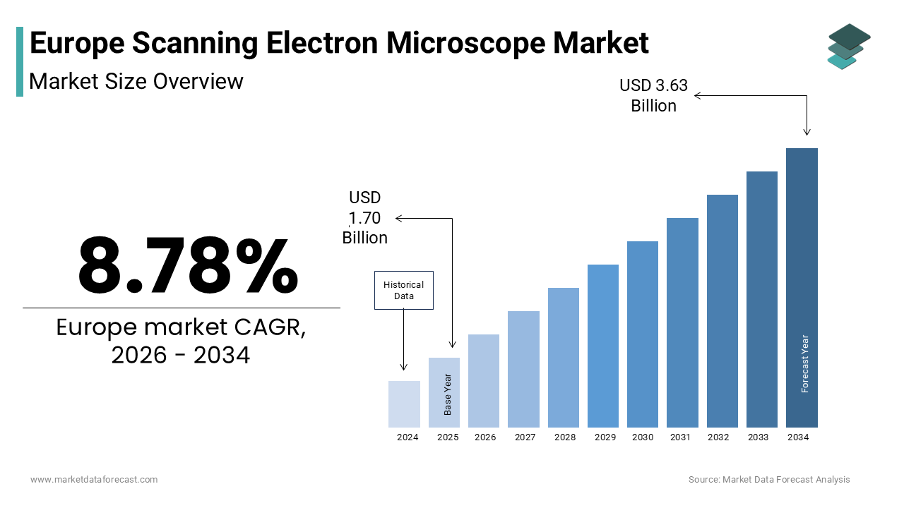
The Europe scanning electron microscope market was valued at USD 1.70 billion in 2025, is anticipated to reach USD 1.85 billion in 2026, and is projected to reach USD 3.63 billion by 2034, growing at a CAGR of 8.78% during the forecast period from 2026 to 2034. The growth of the Europe scanning electron microscope market is primarily driven by rising investments in nanotechnology and advanced materials research, expanding semiconductor and microelectronics manufacturing, and strong public funding for scientific infrastructure across the European Union. Increasing adoption of high-resolution field emission SEMs, growing integration of SEM-based inspection in semiconductor fabrication, and the expansion of open-access research facilities are further supporting market expansion. Additionally, the convergence of artificial intelligence, automated image analysis, and digital microscopy workflows is enhancing productivity and broadening SEM adoption beyond traditional research environments.
Key Market Dynamics
- Expansion of nanotechnology, materials science, and life science research across Europe is sustaining long-term demand for advanced electron microscopy.
- European semiconductor sovereignty initiatives, supported by the European Chips Act, are accelerating SEM adoption for critical dimension metrology and defect analysis.
- High capital and operating costs continue to restrict access for smaller institutions and early-stage companies.
- Dual-use export controls and regulatory compliance requirements are increasing procurement complexity and lead times.
- AI-driven image analysis and automation are emerging as key differentiators, transforming SEMs into intelligent analytical platforms.
Segmental Insights
- By Type, the conventional SEM segment dominated the Europe scanning electron microscope market in 2025, supported by its superior resolution, analytical versatility, and indispensable role in semiconductor failure analysis and advanced materials research. These systems remain central to high-end research institutions and industrial pilot lines where performance outweighs cost and footprint considerations.
- The benchtop SEM segment is expected to register the fastest CAGR, driven by the democratization of electron microscopy across teaching laboratories, SMEs, forensic science, food safety, and cultural heritage applications. Improved user-friendly software, compact design, and automated workflows are expanding adoption beyond traditional microscopy specialists.
- By application, materials science held the largest share of the market, owing to SEM’s critical role in metallurgy, composites, corrosion analysis, and regulatory testing. The semiconductor application segment is projected to witness the fastest growth, fueled by chip manufacturing expansion, advanced packaging, and heterogeneous integration initiatives across Europe.
- By end user, research institutes accounted for the largest market share, reflecting Europe’s coordinated public research funding, national microscopy platforms, and open-access infrastructure models. Meanwhile, the industrial end-user segment is expected to grow at the fastest pace, as manufacturers increasingly integrate SEMs into in-house quality control, failure analysis, and compliance workflows.
Regional Insights
- Germany led the Europe scanning electron microscope market in 2025, supported by its dense research infrastructure, strong industrial base, and leadership in materials science and semiconductor R&D.
- The United Kingdom followed, driven by world-class academic institutions, life sciences investment, and national metrology capabilities.
- France maintains a strong position through centralized research governance, aerospace demand, and microelectronics initiatives.
- The Netherlands plays a strategically important role due to its semiconductor ecosystem, advanced research hubs, and high utilization of electron microscopy in nanotechnology and health tech.
- Switzerland continues to emerge as a high-intensity innovation market, supported by precision industries, elite research institutions, and regulatory agility.
Competitive Landscape
Competition in the Europe scanning electron microscope market is technology-driven and highly consolidated, with leading players differentiating through resolution performance, analytical integration, AI-enabled software, and application-specific workflows rather than price. Market leaders are strengthening their positions by aligning with European research agendas, semiconductor roadmaps, and open science initiatives, while also expanding service, training, and compliance support across the region. Entry barriers remain high due to capital intensity, regulatory scrutiny, and the need for scientific validation, favoring established manufacturers with strong European footprints. Key players operating in the Europe scanning electron microscope market include Carl Zeiss AG, Thermo Fisher Scientific, JEOL Ltd., Hitachi High-Tech Corporation, Leica Microsystems, Tescan Orsay Holding, Bruker Corporation, DELONG Instruments, Nikon Corporation, and Olympus Corporation.
 Download Free Sample Report
Europe Scanning Electron Microscope Market Size
The europe scanning electron microscope market size was valued at USD 1.70 billion in 2025 and is anticipated to reach USD 1.85 billion in 2026 from USD 3.63 billion by 2034, growing at a CAGR of 8.78% during the forecast period from 2026 to 2034.
A Scanning Electron Microscope (SEM) is a powerful scientific instrument that uses a focused beam of electrons instead of light to produce high-resolution, three-dimensional images of a specimen's surface. These capabilities are critical for research in nanotechnology, materials science, life sciences, and semiconductor development. Europe’s scientific infrastructure provides a robust foundation for this market. An extensive network of public laboratories and specialized core facilities operates throughout the European Union to provide advanced microscopy capabilities. According to Eurostat, European Union investment in research and development has continued to grow, with the total expenditure and intensity remaining stable relative to the gross domestic product. Furthermore, the European Research Council funded hundreds of new, high-quality frontier science projects in 2023, with a significant number of these studies requiring advanced imaging at the nanometer scale. These institutional commitments establish a sustained demand environment where scanning electron microscopes function not as optional tools but as essential gateways to scientific discovery and industrial innovation across the continent.
MARKET DRIVERS
Expansion of Nanotechnology and Advanced Materials Research
The region’s strategic focus on nanotechnology and next generation materials is a primary driver of the Europe scanning electron microscope market. The European Commission’s Horizon Europe program prioritizes funding for research into advanced materials, particularly for battery technology, catalysts, and lightweight composites, through its digital and climate-focused clusters. These projects require precise morphological and elemental characterization only achievable through scanning electron microscopy coupled with energy dispersive X ray spectroscopy. Field emission scanning electron microscopy remains the primary technique utilized for material characterization and quality analysis in European nanomaterial research studies. National initiatives amplify this demand. Germany’s Federal Ministry of Education and Research continues to support young researchers in material sciences, facilitating the acquisition of advanced analytical equipment for university research groups. Similarly, The French National Research Agency is investing in advanced cryo-scanning electron microscopy platforms, strengthening the capacity for soft matter analysis at research institutions. These coordinated investments ensure that advanced microscopy remains integral to Europe’s ambition to lead in sustainable materials innovation—directly fueling instrument procurement and technical service demand.
Integration of Scanning Electron Microscopy in Semiconductor and Microelectronics Development
The resurgence of European semiconductor sovereignty initiatives has intensified demand for high precision SEMs in microelectronics fabrication and failure analysis, and thereby propels the expansion of the Europe scanning electron microscope market. The European Chips Act committed billions of euros to strengthen the continent’s semiconductor ecosystem including the construction of new fabrication facilities in Germany, France, and Italy. These fabs require in line and off line scanning electron microscopes for critical dimension metrology defect inspection and process control at nodes below 28 nanometers. The adoption of electron beam inspection technology for pilot manufacturing, particularly within the European semiconductor sector, appears to be increasing. Advanced inspection and imaging systems are being integrated into expanded wafer production facilities to support process development. Research centers in Europe are experiencing higher utilization of microscopy tools, driven by collaborative development initiatives with industry partners. Semiconductor manufacturers are utilizing advanced focused ion beam systems for circuit editing and analysis in their production environments. Europe’s push for semiconductor autonomy necessitates a long-term reliance on advanced electron microscopy, positioning it as an essential quality assurance standard within the regional value chain.
MARKET RESTRAINTS
High Capital and Operational Costs Limit Accessibility for Smaller Institutions
The significant financial burden associated with acquiring and maintaining SEMs restricts their adoption to well-funded research centers and multinational corporations, which limits overall growth in the Europe scanning electron microscope market. Purchasing new field emission electron microscopes requires significant capital investment, with prices varying heavily based on resolution and functionality, often exceeding a million euros for specialized dual-beam or cryogenic setups. Public universities in Southern and Eastern Europe have reduced acquisitions of new electron microscopy equipment due to limited funding, favoring shared regional facilities over individual ownership. Operational expenses further compound the challenge. Annual service contracts are expensive and require stable power supplies vibration free environments and liquid nitrogen or compressed air infrastructure. Due to the high cost of ownership, many Romanian research institutes rely on shared regional laboratory facilities for accessing high-end microscopy, rather than purchasing their own equipment. Even in wealthier nations small biotech startups often lack dedicated microscopy budgets. Early-stage deep tech companies frequently utilize national open-access platforms to access scanning electron microscopes, avoiding the prohibitive cost of direct purchasing and maintenance. This economic stratification risks concentrating advanced analytical capability in a narrow set of institutions thereby constraining broader scientific participation and market penetration.
Complex Regulatory and Export Control Frameworks Delay Deployment
Stringent dual-use export controls and technical regulations in Europe are complicating procurement and cross-border collaboration for SEMs, which impedes the expansion of the Europe scanning electron microscope market. These strict measures require compliance with EU Regulation 2021/821, impacting the trade of high-tech imaging tools. Scanning electron microscopes equipped with high resolution imaging or focused ion beam capabilities are classified under EU Regulation 2021 821 on dual use items due to potential application in nuclear or defense related research. Exporting these instruments to destinations outside the European Union requires individual authorization involving significant, consistent approval timeframes. The transfer of these instruments to non-civilian users within the European Union is subject to mandatory notification procedures. These regulatory requirements, including documentation procedures, have introduced complexities that can influence the speed of commercial transactions and academic collaborations. Shipments of instruments intended for research institutions in neighboring European countries have experienced delays frequently associated with the completion of end-user documentation. Updated product compliance standards now mandate that manufacturers incorporate specific cybersecurity and data integrity features, requiring adjustments to software architecture for networked equipment. These compliance burdens increase lead times inflate costs and create uncertainty particularly for SMEs lacking dedicated regulatory teams, ultimately slowing technology adoption and market fluidity across the region.
MARKET OPPORTUNITIES
Adoption of Artificial Intelligence for Automated Image Analysis
The integration of artificial intelligence into scanning electron microscopy workflows offers strong potential to enhance throughput accuracy, accessibility, and the growth of the Europe scanning electron microscope market. AI algorithms can now automatically detect defects segment microstructures and quantify particle size distributions, tasks that previously required hours of manual analysis by highly trained personnel. Public-private partnerships are funding pilot projects that deploy deep learning models on scanning electron data for material analysis. Research institutions are demonstrating that custom neural networks can reduce the time needed for classifying microstructures in materials. Manufacturers are integrating embedded AI solutions into imaging equipment to enable real-time particle analysis. Initiatives are providing AI microscopy training to smaller laboratories, enabling them to improve the utilization of existing instruments. This convergence of machine learning and electron optics not only democratizes advanced analysis but also creates new software driven revenue streams that redefine the value proposition of scanning electron microscopes beyond hardware.
Growth of Open Access and Shared Research Infrastructure Networks
The expansion of coordinated shared microscopy facilities across the region is opening broader access and fostering collaborative innovation in scanning electron microscopy, and ultimately contributes to the expansion of the Europe scanning electron microscope market. Designated European electron microscopy platforms are recognized as central components for long-term research support. These collaborative networks facilitate access to equipment, training, and data services for diverse research teams. Major imaging consortia are enabling widespread, multi-national utilization of scanning electron microscopy. National initiatives are strengthening capabilities by updating centers with advanced technologies for regional use. Furthermore, virtual portals are being implemented to improve access to national imaging infrastructures. These shared models reduce duplication lower entry barriers and maximize utilization, turning high cost instruments into community resources. Shifting from ownership to access-based infrastructure broadens the user demographic while driving continuous demand for technical assistance and system enhancements in Europe.
MARKET CHALLENGES
Shortage of Skilled Personnel to Operate and Interpret Advanced Microscopy Data
A serious gap persists in the availability of trained professionals who can effectively operate SEMs and interpret complex imaging data across the region, despite technological advancements, which poses a great challenge to the Europe scanning electron microscope market. These instruments demand expertise in vacuum systems electron optics sample preparation and analytical spectroscopy, skills not uniformly covered in standard curricula. Observations indicate a notable shortage of certified electron microscopy professionals across various European regions, with particular concentration in the southern and eastern areas. Analysis suggests that specialized training for electron microscopy is not heavily featured in materials science curricula, and the current academic pipeline is considered insufficient to meet demand. This skills mismatch leads to suboptimal instrument usage extended turnaround times and over reliance on vendor support, increasing operational costs. Europe's scientific competitiveness and the expansion of its scanning electron microscope (SEM) market are at risk due to underutilized infrastructure, driven by a lack of coordinated training and technical talent mobility.
Rapid Technological Obsolescence and Fragmented Interoperability Standards
The accelerating pace of innovation in electron optics software and detectors is creating barriers related to technological obsolescence and data interoperability that negatively impact the expansion of the Europe scanning electron microscope market. Instruments purchased just five years ago often lack compatibility with modern AI driven analysis tools cloud data storage or automated stage control systems. Many educational and research institutions continue to rely on older operating systems for microscope functionality, which complicates direct integration with modern laboratory information management platforms. Furthermore, the absence of universal data formats impedes collaboration. Scanning electron image data often requires specific, vendor-provided conversion tools to be usable within open-source analysis software. This fragmentation discourages data sharing and reproducibility, core principles of the European Open Science Cloud. Additionally, Manufacturer support for older hardware models tends to cease after a set period, frequently necessitating complete equipment replacements for research facilities. These dynamics create financial and technical instability particularly for public laboratories with fixed capital budgets, ultimately constraining long term planning and sustainable adoption of advanced microscopy technologies in the European research ecosystem.
REPORT COVERAGE
| REPORT METRIC | DETAILS |
| Market Size Available | 2025 to 2034 |
| Base Year | 2025 |
| Forecast Period | 2026 to 2034 |
| CAGR | 8.78% |
| Segments Covered | By Type, Application, End-User and Region |
| Various Analyses Covered | Regional & Country Level Analysis, Segment-Level Analysis, DROC, PESTLE Analysis, Porter’s Five Forces Analysis, Competitive Landscape, Analyst Overview on Investment Opportunities |
| Countries Covered | UK, France, Spain, Germany, Italy, Russia, Sweden, Denmark, Switzerland, the Netherlands, Turkey, the Czech Republic, and the Rest of Europe. |
| Market Leaders Profiled | Carl Zeiss AG, Thermo Fisher Scientific, JEOL Ltd., Hitachi High-Tech Corporation, Leica Microsystems, Tescan Orsay Holding, Bruker Corporation, DELONG Instruments, Nikon Corporation, and Olympus Corporation. |
SEGMENTAL ANALYSIS
By Type Insights
In 2025, the conventional SEMs segment dominated the Europe scanning electron microscope market by accounting for a substantial share. The dominance of the conventional SEMs segment is driven by its unparalleled resolution depth of field and analytical versatility which are essential for advanced research and industrial quality control. An additional driver of this segment is its irreplaceable role in semiconductor failure analysis and materials characterization where sub nanometer imaging is non-negotiable. European microelectronics pilot lines and failure labs are increasingly adopting advanced field emission scanning electron microscopes to support nanometer-scale imaging of next-generation devices. These systems enable critical dimension metrology defect localization and cross sectional imaging at nodes below 10 nanometers, capabilities benchtop models cannot replicate. Furthermore, national research infrastructures prioritize conventional systems. Key European research infrastructure landmarks are consolidating advanced electron microscopy capabilities, incorporating in situ and cryo techniques to facilitate high-level scientific research. This institutional anchoring ensures sustained procurement for core scientific missions where performance trumps footprint or cost. Also supporting this segment is the integration of conventional systems into multimodal analytical platforms. Modern conventional scanning electron microscopes are routinely coupled with focused ion beams energy dispersive X ray spectrometers and electron backscatter diffraction detectors creating comprehensive materials interrogation workstations. Advanced metallurgy projects at the Max Planck Institute for Iron Research depend heavily on simultaneous electron backscatter diffraction and energy dispersive spectroscopy mapping to characterize microstructural features. Similarly, the European Space Agency’s Materials and Electrical Components Laboratory in the Netherlands relies on conventional systems for radiation damage assessment of spacecraft alloys. These mission critical applications demand the highest beam coherence vacuum integrity and stage precision, attributes engineered into conventional designs over decades. Europe’s progress in fusion and quantum tech keeps traditional analytical tools dominant, despite the growing availability of smaller, compact options.
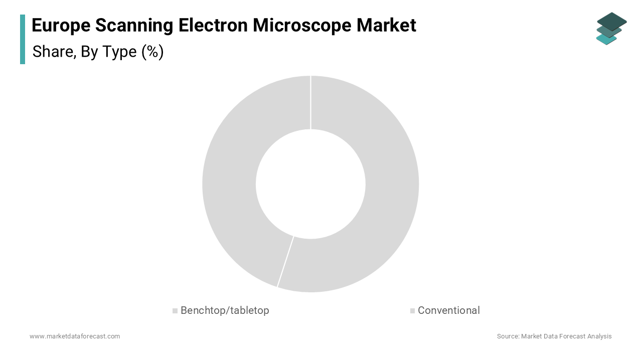
The benchtop or tabletop SEM segment is predicted to witness the highest CAGR of 9.3% from 2026 to 2034 due to democratization of electron microscopy in non traditional settings. Unlike conventional systems benchtop SEMs require no dedicated facility vibration isolation or high voltage infrastructure making them deployable in teaching labs small factories and clinical environments. A further booster is their adoption in vocational education and applied sciences. Academic and research institutions across Germany, France, and the Netherlands have increased their adoption of user-friendly desktop scanning electron microscopes to enhance material characterization capabilities in teaching and research. These instruments typically deliver 10 to 20 nanometer resolution, sufficient for quality control in metallography polymer analysis and particle sizing. In the industrial sector small and medium enterprises in the automotive and packaging sectors use them for rapid root cause analysis without outsourcing. Small and medium-sized enterprises (SMEs) within the Baden-Württemberg engineering sector are increasingly adopting in-house benchtop SEMs for rapid, on-site failure diagnosis and quality control. In addition, a top factor is the integration of user friendly software and automated workflows that minimize operator dependency. Modern benchtop systems from Thermo Fisher Hitachi and Phenom feature touchscreen interfaces one click imaging and AI assisted particle analysis compliant with EU data standards. This ease of use has opened new applications in forensic science food safety and cultural heritage. Portable analytical equipment allows for detailed, non-invasive examinations directly at the site of the object or material, reducing the need for sample removal. Modern, compact instrumentation has expanded access to high-level analysis, facilitating localized monitoring and improving efficiency in scientific workflows. These cross sectoral use cases demonstrate how compact electron microscopy is transitioning from a specialist tool to a routine analytical asset, expanding the total addressable market beyond traditional research confines and fueling its status as Europe’s highest growth segment.
By Application Insights
The material science segment was the largest segment in the Europe scanning electron microscope market by 38.2% share in 2025. The prominence of the material science segment is attributed to its foundational role in metallurgy ceramics composites and failure analysis across industrial and academic domains. Scanning electron microscopy is indispensable for characterizing grain structure fracture surfaces phase distribution and corrosion mechanisms, tasks critical to product reliability and innovation. Also helping this segment grow is Europe’s leadership in advanced manufacturing and green materials. Organizations are increasingly adopting portable imaging and analysis technologies to study delicate or restricted items directly on-site, eliminating the need for transport. Field-deployable systems allow for the in-depth examination of cultural artifacts and the analysis of material degradation without removing samples from their collections. Furthermore, specialized analytical techniques are being utilized for rapid inspection and contamination analysis in food safety applications, enabling, for example, the assessment of fine particles in consumer products at the point of testing. Overall, there is a shift toward decentralizing research, allowing for specialized material analyses in the field rather than relying solely on dedicated, off-site laboratory facilities. These industrial and research imperatives make material science the most consistent and volume intensive application for scanning electron microscopes across the continent. This segment is further supported by the integration of electron microscopy into regulatory and certification frameworks. Regulatory bodies are increasingly incorporating scanning electron microscopy as a standard method for investigating fatigue failure in aviation components. The European Committee for Standardization utilizes microstructural documentation, often involving high-resolution imaging, to ensure compliance with pressure equipment regulations. Environmental and chemical safety guidelines are evolving to include particulate morphology, driving the use of electron imaging for analyzing additives in polymer materials. These regulatory anchors convert scientific capability into mandatory practice. Furthermore the rise of circular economy models demands material traceability. The Fraunhofer Institute for Recycling Technology uses SEM energy dispersive spectroscopy to identify alloy compositions in end-of-life vehicles enabling high purity scrap sorting. This convergence of innovation regulation and sustainability ensures that material science remains the bedrock application for electron microscopy in Europe’s industrial and scientific ecosystem.
The semiconductor application segment is estimated to register the fastest CAGR of 11.7% during the forecast period owing to the continent’s strategic push for chip sovereignty and advanced microelectronics. European initiatives are directing significant resources toward expanding regional semiconductor manufacturing capabilities and constructing new production facilities. The newly established facilities require advanced scanning electron microscopy technology for critical dimension metrology, defect inspection, and process control. There is a notable increase in the installation of electron beam inspection tools within European semiconductor pilot lines to support advanced technology nodes. Major European manufacturers are enhancing their production capacities, particularly for specialized technologies like silicon carbide devices, by increasing their high-throughput electron microscopy tools. The expansion efforts are resulting in a substantial upgrade of semiconductor inspection infrastructure to enhance process control and production capability. This industrial renaissance transforms SEMs from research instruments into essential production line assets. Growth is further pushed by the expansion of research collaboration around advanced packaging and heterogeneous integration. The IMEC research hub in Belgium leads the European Processor Initiative developing 3D stacked chips that require precise cross sectional imaging of through silicon vias and microbumps, tasks exclusively performed by dual beam focused ion beam scanning electron microscopes. Collaborative projects between research institutions and industry partners have led to increased utilization of scanning electron microscopy for chip development. Initiatives in Europe are supporting the creation of pilot lines focused on advanced computing technologies, including neuromorphic and quantum architectures. Validation processes for these specialized chips are incorporating high-resolution scanning electron microscopy. Europe’s push for chip independence through joint public-private funding is driving sustained demand for advanced electron microscopy, making semiconductors the market's fastest-growing segment.
By End User Insights
The research institutes segment led the Europe scanning electron microscope market by occupying a 52.6% share in 2025. The supremacy of the research institutions segment is credited to Europe’s coordinated research funding framework. These institutions, including national laboratories universities and transnational research infrastructures, serve as the primary hubs for advanced electron microscopy due to their mission of fundamental discovery and method development. Frontier science research increasingly incorporates high-resolution electron imaging across diverse fields such as nanomaterials, life sciences, and geosciences. National investments are actively supporting the proliferation of dedicated microscopy centers and the integration of scanning electron microscopes. Research institutions are forming interdisciplinary teams to utilize specialized imaging infrastructure. Advanced imaging facilities are combining electron microscopy with other techniques, such as synchrotron light sources, to enable correlative studies. Scientific infrastructure is evolving to provide open-access, remote imaging capabilities to external users, supporting broader research collaboration. This open science model maximizes utilization and justifies ongoing capital renewal. Besides, the segment benefits from the role of research institutes in developing next generation methodologies that push instrumental boundaries. Projects in cryo electron tomography in situ heating and gas environmental SEM originate in academic labs before commercialization. Research institutions have refined scanning electron microscopy techniques to better observe materials that are easily damaged by traditional imaging methods. These advancements allow for the examination of delicate structures without compromising their integrity during the analysis process. The innovations keep research institutes at the technological forefront requiring continuous instrument refresh. Furthermore, Horizon Europe’s emphasis on interdisciplinary collaboration, such as merging materials science with AI or biomedicine, demands versatile SEM platforms with multimodal capabilities. This dual role as both user and innovator ensures research institutes remain the dominant and most sophisticated end user segment in the European scanning electron microscope landscape.
The industrial end user segment is anticipated to witness the fastest CAGR of 10.2% from 2026 to 2034. The rapid expansion of the industrial end user segment is propelled by vertical integration of quality control and failure analysis across high value manufacturing sectors. Companies in automotive aerospace medical devices and electronics are increasingly bringing electron microscopy in house to accelerate root cause analysis and reduce reliance on external labs. Industrial organizations are increasingly investing in automated scanning electron microscopy to support predictive maintenance and enhance quality control. The integration of these tools into production lines enables rapid, real-time inspection of components, resulting in faster defect resolution. A further booster of this segment is the rise of advanced materials in industrial products. The rising market share of EV lightweight alloys and bioresorbable implants makes SEM-based verification of microstructural integrity critical for performance. Regulatory bodies are increasingly requiring comprehensive analysis of surface characteristics and particulate data for implantable devices, leading to greater utilization of imaging technologies for compliance submissions. Medical device manufacturers are strengthening their quality control capabilities by increasing the number of electron microscopy systems to analyze surface coatings and textures. New environmental regulations for battery technologies necessitate detailed reports on particle size, encouraging manufacturers to incorporate automated microscopy-based quality checks directly into production lines. These regulatory and material shifts transform SEMs from optional R and D tools into mandatory production line assets. Reshoring is sparking a tech revolution in Europe: in-house electron microscopy is booming, turning industrial applications into the market's ultimate growth vector.
REGIONAL ANALYSIS
Germany Scanning Electron Microscope Market Analysis
Germany was the top performer in the Europe scanning electron microscope market by accounting for a 24.6% share in 2025. The leading position of the German market is supported by its status as the continent’s scientific and industrial powerhouse. The country’s market status is also driven by dense research infrastructure world class engineering firms and strong public investment in advanced manufacturing. Research institutions and universities are prioritizing significant investments in high-end imaging equipment to upgrade their technical capabilities. The deployment of advanced scanning electron microscopes is accelerating across both academic and research centers. Industrial sectors, particularly in manufacturing and technology, show a strong, consistent demand for specialized microscopy for analysis and testing purposes. There is a notable trend of increased adoption of scanning electron microscopes in automotive and semiconductor industries for quality assurance. Major hubs like Dresden Stuttgart and Berlin host clusters where companies such as Zeiss Bosch and Infineon collaborate with institutes like Fraunhofer and Max Planck on quantum materials and chip development, activities inherently dependent on high end microscopy. This synergy of public science and private industry creates a self reinforcing ecosystem that sustains Germany’s leadership in both adoption and technological advancement of electron microscopy.
United Kingdom Scanning Electron Microscope Market Analysis
The United Kingdom was the second largest country in the Europe scanning electron microscope market by capturing a 18.9% share in 2025. The growth of the UK market is fuelled by its globally recognized academic institutions, strategic life sciences investments, and sustained funding through UK Research and Innovation. Investment is being directed toward upgrading national research infrastructure, with a particular focus on advanced imaging, materials science, and synchrotron capabilities. Key academic institutions are maintaining and operating sophisticated, high-end electron microscopy and imaging facilities, which support international research collaborations. Following changes to regional partnerships, there is an increased focus on strengthening domestic capabilities in health, diagnostics, and vaccine development. The emphasis on health and security is driving demand for advanced imaging technologies essential for nanoparticle analysis and virus characterization. Furthermore, the National Physical Laboratory uses SEMs for nanometrology standards ensuring traceability across industrial sectors. This combination of academic prestige strategic autonomy and metrological leadership ensures the UK remains a high value and high intensity market for advanced electron microscopy.
France Scanning Electron Microscope Market Analysis
France maintains a significant share of the Europe scanning electron microscope market due to national sovereignty initiatives in quantum computing microelectronics and aerospace. The country’s market status is shaped by centralized research governance through organizations like CNRS and CEA which operate several national microscopy platforms. National research strategies are prioritizing the acquisition of advanced microscopic instrumentation to support emerging energy and microelectronics sectors. Governmental initiatives are increasingly focusing on specialized imaging tools to advance development in energy storage and semiconductor technologies. Regional legislative frameworks aimed at strengthening domestic electronics ecosystems are facilitating the expansion of manufacturing capabilities. Strategic investments in high-throughput analytical equipment allow for the production of sophisticated microelectronics components within competitive global markets. The aerospace industry relies on precise microscopy to conduct critical material inspections that ensure components meet rigorous safety and airworthiness standards. There is a clear pattern of integrating high-resolution surface analysis into industrial certification processes to validate the durability of engine components. Paris Saclay and Grenoble serve as innovation poles where public private partnerships accelerate technology transfer. This top down coordination ensures consistent funding cycles and standardization that favor long term electron microscopy investment—cementing France’s position as a strategic leader in applied microscopy.
Netherlands Scanning Electron Microscope Market Analysis
The Netherlands occupies a noteworthy position in the Europe scanning electron scanning microscope market owing to its concentration of global technology leaders and advanced research hubs. The country’s market status is uniquely defined by the presence of ASML Philips and the IMEC Netherlands collaboration which position electron microscopy as critical to semiconductor and health tech innovation. Research and development facilities are heavily employing advanced imaging tools like scanning electron microscopes for the advancement of microchip technology. A significant portion of research instrumentation funding is being directed toward electron and ion beam platforms to support the development of nanotechnology and quantum materials. Surface analysis technologies, including scanning electron microscopes, are being applied to analyze sustainable packaging and materials as part of broader environmental initiatives. Furthermore, the country’s compact geography enables rapid service and training networks ensuring high instrument uptime. This ecosystem of global corporate presence elite research and logistical efficiency makes the Netherlands a disproportionate influencer in Europe’s high end microscopy landscape.
Switzerland Scanning Electron Microscope Market Analysis
Switzerland is expected to account for a prominent share of the European scanning electron microscope market over the forecast period owing to its concentration of world leading research institutions and precision industries. The country’s market status is anchored by ETH Zurich EPFL and the Paul Scherrer Institute which operate some of the most advanced in situ and cryo electron microscopy facilities in Europe. Industrial demand comes from medical device and watchmaking sectors where microstructural perfection is non negotiable. Companies like Roche and Swatch Group use SEMs for nanoparticle drug characterization and gear surface inspection respectively. Furthermore Switzerland’s non EU but EFTA aligned status allows rapid adoption of cutting edge technologies without regulatory lag. This fusion of academic excellence industrial precision and regulatory agility ensures Switzerland remains a high intensity and innovation driven node in the Europe scanning electron microscope market.
COMPETITIVE LANDSCAPE
Competition in the Europe scanning electron microscope market is defined by a technologically intense yet consolidated landscape where global leaders compete on performance innovation and ecosystem integration rather than price. Companies such as Thermo Fisher ZEISS and Hitachi differentiate through resolution speed analytical versatility and software intelligence rather than hardware alone. The market rewards those who provide end to end solutions including application support data compliance training and service not just instruments. While entry barriers remain high due to capital intensity regulatory complexity and required scientific validation smaller players focus on niche segments like benchtop systems or specialized detectors. Competition is further shaped by Europe’s strategic emphasis on semiconductor sovereignty quantum materials and open science which demand cutting edge microscopy as a foundational capability. In this environment leadership is sustained through deep alignment with public research agendas industrial quality needs and digital governance frameworks making the market a nexus of science policy and precision engineering.
KEY MARKET PLAYERS
Some of the companies that are playing a dominating role in the Europe Scanning Electron Microscope Market include
- Carl Zeiss AG
- Thermo Fisher Scientific
- JEOL Ltd.
- Hitachi High-Tech Corporation
- Leica Microsystems
- Tescan Orsay Holding
- Bruker Corporation
- DELONG Instruments
- Nikon Corporation
- Olympus Corporation
Top Players in the Europe Scanning Electron Microscope Market
Thermo Fisher Scientific
Thermo Fisher Scientific is a dominant force in the Europe scanning electron microscope market through its advanced field emission and dual beam platforms under the FEI and Helios brands. The company actively supports academic hospitals and semiconductor research centers across the continent with localized application specialists and compliance expertise. It also expanded its sustainable lab initiative by introducing energy efficient vacuum systems compliant with EU Ecodesign standards. Globally Thermo Fisher leverages its European innovations in cryo and in situ SEM to set benchmarks adopted in North American and Asian semiconductor and life science hubs reinforcing its role as a technology leader in high resolution electron optics.
ZEISS Group
ZEISS Group exerts significant influence in the Europe scanning electron microscope market through its integrated portfolio of electron and ion beam systems tailored for materials science and industrial metrology. Headquartered in Germany the company maintains deep collaborations with automotive aerospace and microelectronics firms requiring precision failure analysis. It also partnered with the Fraunhofer Institute to develop low voltage SEM protocols for beam sensitive polymers used in medical devices. Globally ZEISS exports its European engineered metrology solutions to semiconductor fabs in Asia and North America where EU derived quality standards are increasingly mandated, solidifying its reputation as a pioneer in industrial electron microscopy.
Hitachi High Technologies Corporation
Hitachi High Technologies maintains a strong presence in the Europe scanning electron microscope market primarily through its benchtop and analytical SEM systems widely adopted in vocational education and small industrial labs. The company emphasizes ease of use automation and compact design making electron microscopy accessible beyond traditional research settings. It also expanded its service network across Southern and Eastern Europe offering remote diagnostics and virtual training. Globally Hitachi leverages its European user feedback to refine entry level platforms deployed in emerging markets where affordability and simplicity drive adoption, positioning Europe as a key innovation and validation hub for democratized electron microscopy
Top Strategies Used by the Key Market Participants
Key players in the Europe scanning electron microscope market prioritize application specific innovation by developing tailored workflows for semiconductors life sciences and advanced materials aligned with EU regulatory and research priorities. They invest in artificial intelligence integration to automate image analysis and reduce dependency on expert operators. Strategic expansion of service and training networks across Southern and Eastern Europe enhances customer retention and instrument uptime. Companies also focus on sustainability by introducing energy efficient vacuum systems and modular designs that support longer lifecycles and easier upgrades. Furthermore they strengthen digital compliance by embedding data governance features that meet EU cybersecurity and health data standards. These strategies collectively reinforce technical leadership operational support and regulatory readiness essential for sustained competitiveness in Europe’s high precision scientific instrumentation landscape.
MARKET SEGMENTATION
This research report on the europe scanning electron microscopes market has segmented and sub-segmented based on categories.
By Type
- Benchtop/tabletop
- Conventional
By Application
- Material Science
- Nanotechnology
- Life Science
- Semiconductors
- Other Applications
By End-User
- Industries
- Research Institutes
- Hospitals
By Country
- UK
- France
- Spain
- Germany
- Italy
- Russia
- Sweden
- Denmark
- Switzerland
- Netherlands
- Turkey
- Czech Republic
- Rest of Europe