Global 3D TSV Market Size, Share, Trends, & Growth Forecast Report By Product (Memory, MEMS, CMOS Image Sensors, Imaging and Optoelectronics, Advanced LED Packaging, and Others), End-Users (Consumer Electronics Sector, Information and Communication Technology Sector, Automotive Sector, Military, Aerospace and Defense, and Others) & Region, Industry Forecast From 2024 to 2033
Global 3D TSV Market Size
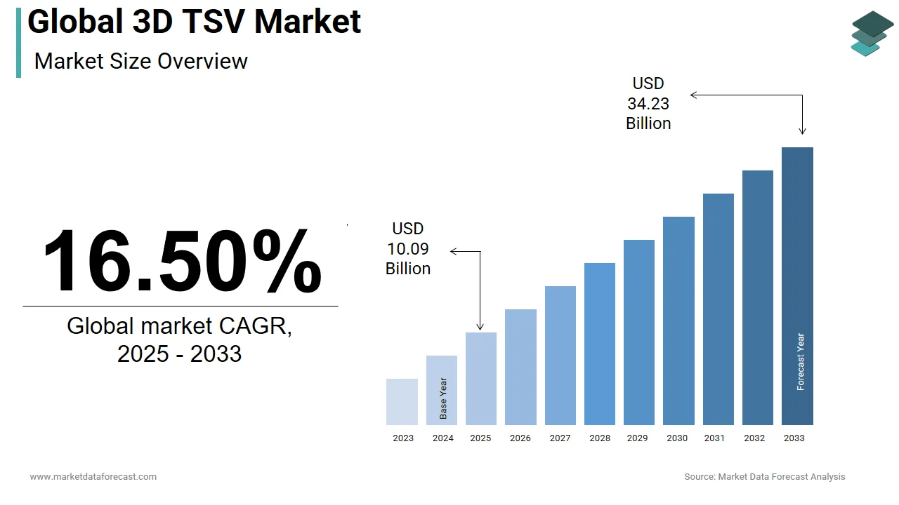
The global 3D TSV market was worth USD 8.66 billion in 2024. The global market is predicted to reach USD 10.09 billion in 2025 and 34.23 billion by 2033, growing at a CAGR of 16.50% during the forecast period 2025 to 2033.
3D TSV devices are a high-performance interconnection technique that passes through a silicon wafer via a vertical electrical connection, reducing power consumption and improving electrical performance. 3D TSV technology enables LSI stacking to facilitate manufacturing smaller products, such as portable devices. To meet increasing demands for functional integration, semiconductor manufacturers are adopting 3D TSV technology around the world.
MARKET DRIVERS
The increasing use of LEDs in products has fostered the creation of devices with higher energy, higher density, and lower cost.
Unlike 2D gaskets, the use of three-dimensional (3D) gaskets through silicon via technology (TSV) allows a high density of vertical interconnections. The growing demand for innovative chip architectures with improved features such as low power consumption, high aspect ratio, and lower form factor is driving the 3D TSV market.
The increasing need for the compactness of electronic devices is driving the expansion of the 3D TSV market. These products can be obtained by integrating hetero systems, which can result in more reliable advanced packaging.
With extremely small MEMS sensors and 3D electronics, the sensors can be placed virtually anywhere, and equipment can be monitored in harsh environments in real-time to help increase reliability and availability. Variables such as the proliferation of cloud-based applications, a strong perspective in information and communication technologies, and continued advancements in the DRAM and smart lighting industries reinforce the acceptance of 3D packages for manufacturing processes. However, thermal problems caused by higher integration levels are restricting the growth of the 3D TSV market.
The increasing use of light-emitting diodes (LEDs) in products has encouraged the development of devices with higher power, higher density, and lower cost. The use of three-dimensional (3D) packaging, thanks to silicon technology (TSV), allows a high density of vertical interconnections, unlike 2D packaging. TSV IC is known to decrease connection lengths, so less capacitance, inductance, and resistance to parasites are needed when an integrated monolithic and multifunctional solution is performed efficiently, which can result in high-speed and low-power interconnects.
A recessed design with thin silicone membranes on the bottom optimizes thermal contact and thus minimizes thermal resistance. The silicon path (TSV) provides electrical contact to surface-mounted devices, and the mirrored sidewalls increase the reflectivity of the housing and improve light efficiency. SUSS AltaSpray technology can coat almost the integration of 90° corners, KOH etched cavities, and TSV varying from a few microns to 600 μm or more. The ability to produce tough and conformal coatings in severe topography, such as TSV, makes it the ideal choice for wafer-level LED packaging, increasing market growth.
REPORT COVERAGE
| REPORT METRIC | DETAILS |
| Market Size Available | 2024 to 2033 |
| Base Year | 2024 |
| Forecast Period | 2025 to 2033 |
| CAGR | 16.50% |
| Segments Covered | By Product, End Users, and Region. |
|
Various Analyses Covered | Global, Regional & Country Level Analysis, Segment-Level Analysis, DROC, PESTLE Analysis, Porter’s Five Forces Analysis, Competitive Landscape, Analyst Overview on Investment Opportunities |
| Regions Covered | North America, Europe, APAC, Latin America, Middle East & Africa |
|
Market Leaders Profiled | Amkor Technology, United Microelectronics Corp, Intel Corporation, Samsung Electronics Co. Ltd, Toshiba Corp, Pure Storage Inc, Broadcom Ltd, Advanced Semiconductor Engineering Inc, Taiwan Semiconductor Manufacturing Company Limited, STMicroelectronics NV, Jiangsu Changing Electronics Technology Co. Ltd, and Others. |
REGIONAL ANALYSIS
Asia-Pacific is also one of the busiest manufacturing centers in the world. The increasing demand for smartphones and the demand for new memory technologies have increased the growth of computer-intensive consumer electronics, creating a wide range of opportunities in this region. Since silicon wafers are widely used to make smartphones, the introduction of 5G technology is expected to boost 5G smartphone sales, which could grow the market in the telecommunications sector.
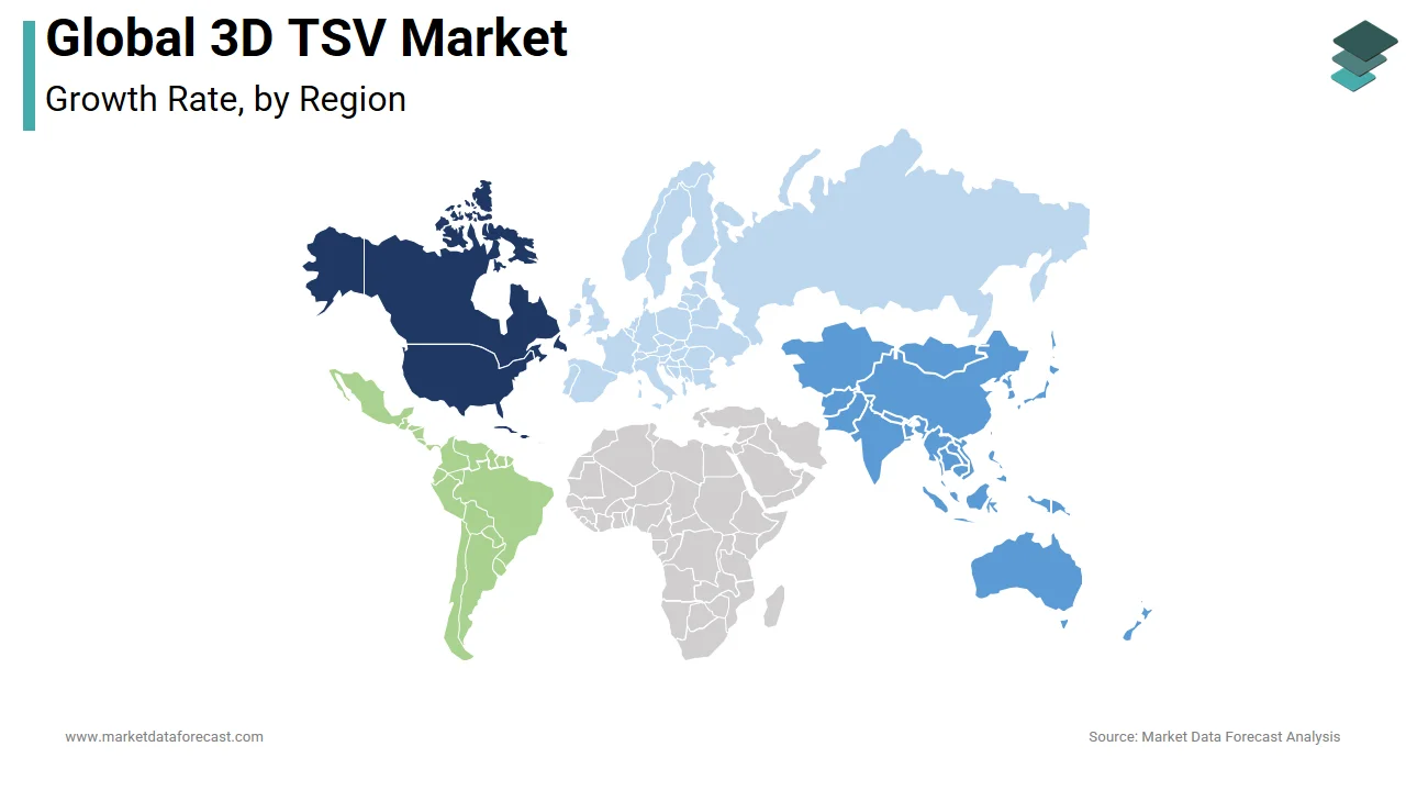
In terms of revenue, Asia-Pacific had the largest market share of the global 3D TSV market in 2017, followed by North America. The main contributors to the growth of the 3D TSV market in the Asia-Pacific region are China, India, and Taiwan due to demand from the consumer electronics, automotive, and transportation industries.
KEY PARTICIPANTS IN THE MARKET
The major companies operating in the global 3D TSV market include Amkor Technology, United Microelectronics Corp., Intel Corporation, Samsung Electronics Co. Ltd., Toshiba Corp., Pure Storage Inc., Broadcom Ltd., Advanced Semiconductor Engineering Inc., Taiwan Semiconductor Manufacturing Company Limited, STMicroelectronics NV, Jiangsu Changing Electronics Technology Co. Ltd., and Others.
RECENT HAPPENINGS IN THE MARKET
-
In October 2019, Samsung started the industry's first 12-layer 3D packaging for the products of DRAM. The technology uses TSVs to create high-capacity, high-bandwidth memory devices for applications such as high-end graphics, FPGAs, and computer cards.
-
In April 2019, TSMC certified ANSYS (ANSS) solutions for its novel System-on-Integrated-chips (SoIC) advanced 3D chip stacking technology. SoIC is an advanced interconnect technology for multi-bay stacking in system-level integration using Through Silicon Via (TSV) and chip-to-wafer bonding process that enables customers to increase the energy efficiency and performance for highly complex and demanding cloud and data center applications.
MARKET SEGMENTATION
This research report on the global 3D TSV market has been segmented and sub-segmented based on the product, end users, and region.
By Product
-
Memory
-
MEMS
-
CMOS Image Sensors
-
Imaging and Optoelectronics
-
Advanced LED Packaging
-
Others
By End-Users
-
Consumer Electronics
-
Information and Communication Technology Industry
-
Automotive Industry
-
Military, Aerospace and Defense Industry
-
Others
By Region
-
North America
-
The United States
-
Canada
-
Rest of North America
-
-
Europe
-
The United Kingdom
-
Spain
-
Germany
-
Italy
-
France
-
Rest of Europe
-
-
The Asia Pacific
-
India
-
Japan
-
China
-
Australia
-
Singapore
-
Malaysia
-
South Korea
-
New Zealand
-
Southeast Asia
-
-
Latin America
-
Brazil
-
Argentina
-
Mexico
-
Rest of LATAM
-
-
The Middle East and Africa
-
Saudi Arabia
-
UAE
-
Lebanon
-
Jordan
-
Cyprus
-
Frequently Asked Questions
How is the 3D TSV market impacted by advancements in semiconductor manufacturing processes?
Continuous advancements in semiconductor manufacturing, such as the transition to smaller nodes and the development of innovative packaging techniques, significantly influence the 3D TSV market, enabling higher integration and improved performance.
What challenges does the 3D TSV market face in terms of adoption and implementation?
Challenges include the high initial investment required for infrastructure setup, concerns related to thermal management, and the need for standardization in the design and manufacturing processes to ensure compatibility.
What technological innovations are shaping the future of 3D TSV technology on a global scale?
Emerging technologies such as through-silicon vias (TSVs) with nanoscale dimensions, advanced materials like silicon interposers, and the integration of heterogeneous devices are key innovations shaping the future of 3D TSV technology.
How does the 3D TSV market respond to the growing demand for 5G-enabled devices worldwide?
The rollout of 5G networks is boosting the demand for 3D TSV technology, as it facilitates the development of compact and high-performance devices capable of handling the increased data speeds and connectivity demands.
Access the study in MULTIPLE FORMATS
Purchase options starting from
$ 2500
Didn’t find what you’re looking for?
TALK TO OUR ANALYST TEAM
Need something within your budget?
NO WORRIES! WE GOT YOU COVERED!
Call us on: +1 888 702 9696 (U.S Toll Free)
Write to us: sales@marketdataforecast.com