- Product Description Description
- Table of Contents TOC
- List of Table & Figure LOT
- Get Free Sample PDF Sample PDF
Market Size, 2025
$7.87 BnMarket Estimate, 2026
$9.01 BnMarket Forecast, 2034
$26.61 BnCAGR, 2026–2034
14.5%Executive Summary: Global Thin and Ultra-thin Films Market
- Market Scope: Comprehensive global analysis of the thin and ultra-thin films market covering material types, deposition techniques, end-user industry verticals, and regional expansion frameworks.
- Market Valuation: Valued at USD 7.87 billion (2025), estimated at USD 9.01 billion (2026), and projected to reach USD 26.61 billion by 2034, registering a robust CAGR of 14.50% (2026–2034).
- Primary Growth Drivers: Proliferation of advanced semiconductor nodes (sub-5nm scaling), expansion of flexible and wearable electronics requiring conformal thin films, and integration into next-generation photovoltaic and quantum computing architectures.
Key Market Segment Metrics (2026–2034)
| Category | Leading Segment (Base Position) | Fastest-Growing Segment |
|---|---|---|
| By Material Type | Inorganic Thin Films (captured a 48.2% share anchored by superior thermal stability, electrical conductivity, and semiconductor/photovoltaic compatibility) | Nanocomposite Thin Films (projected at the fastest CAGR of 12.4% driven by multifunctional performance and flexible OLED barrier applications) |
| By Deposition Techniques | Physical Vapor Deposition (PVD) (held the largest share of 36.2% due to versatility, high deposition rates, and metallic/ceramic compatibility) | Atomic Layer Deposition (ALD) (projected at the fastest CAGR of 14.1% fueled by unmatched conformality and sub-angstrom control) |
| By End-User Industry | Semiconductor (held a 42.5% share as thin films are fundamental to transistor gate stacks, interconnects, and advanced 3D packaging) | Medical and Biomedical Applications (expected to exhibit a noteworthy CAGR of 13.8% driven by implantable electronics and diagnostics) |
| By Region / Country | Asia Pacific (top performer accounting for 45.5% share backed by semiconductor manufacturing concentration and consumer electronics hubs) | North America & Europe (strong leadership in semiconductor design, quantum research, advanced equipment, and specialty chemicals) |
Major Market Players & Market Structure
Market Structure: Highly competitive, capital-intensive global landscape featuring vertically integrated equipment manufacturers, specialty chemical suppliers, and materials innovators competing on atomic precision, defect density control, and application expertise.
Key Companies: Applied Materials Inc., Merck KGaA, ULVAC Inc., Orange Thin Films, American Elements, ThinFilms Inc., LEW Techniques Ltd, Angstrom Engineering Inc., Denton Vacuum, Super Conductor Materials, Inc., Kaneka Corporation, Arrow Thin Films, Inc., Umicore, Plasma-Therm, Materion Corporation, Intevac, Inc., AIXTRON, GEOMATEC Co., Ltd., Kurt J. Lesker Company, PVD Products, Inc., Vital Materials Co., Limited, Praxair S.T. Technology, Inc., and AJA International, Inc.
Global Thin and Ultra-thin Films Market Size
The Global Thin and Ultra-thin Films Market is projected to grow from USD 7.87 billion in 2025 to USD 9.01 billion in 2026 and reach USD 26.61 billion by 2034, registering a CAGR of 14.50% from 2026 to 2034.
Thin and ultra-thin films refer to engineered layers of material ranging from a few nanometers to several micrometers in thickness, deposited onto substrates to impart specific optical, electrical, thermal, or barrier properties. These films are foundational to modern microelectronics, photovoltaics, flexible displays, and advanced packaging technologies. Unlike bulk materials, their functionality arises from quantum confinement surface effects and precise stoichiometry control. According to various sources, critical transistor gate oxides in advanced semiconductor nodes utilize ultra-thin high-k dielectric films. As per research, most semiconductor manufacturing processes rely significantly on thin-film deposition steps. Specialized ultra-thin optical coatings are essential for precise performance on sensitive equipment like satellite sensors. Furthermore, high-efficiency solar cell technology incorporates ultra-thin charge transport layers to achieve advanced performance metrics. These technical benchmarks illustrate how performance frontiers across multiple high-tech domains are increasingly defined by nanoscale film engineering rather than bulk material selection.
MARKET DRIVERS
Proliferation of Advanced Semiconductor Nodes Drives Ultra-Thin Film Adoption
The relentless scaling of integrated circuits below the five-nanometer node necessitates atomic-level precision in dielectric and conductive film deposition, which directly fuels the growth of the thin and ultra-thin films market. The semiconductor industry uses high-k dielectrics, specifically hafnium oxide, as a replacement for silicon dioxide in increasingly small transistors to mitigate the significant leakage currents that occur at thicknesses below 2 nm. According to sources, manufacturing capacity for advanced logic chips (sub-three-nanometer) is anticipated to see significant expansion over the next few years. Industry-wide measurement protocols for ensuring consistent film thickness across semiconductor wafers are established, requiring minimal deviation. Achieving reliable copper interconnects in advanced chip nodes relies on the application of specific, extremely thin barrier layers to manage material behavior. As per studies, the progression to newer logic nodes generally involves an increase in the total number of thin-film deposition steps required to build an advanced chip. This geometric complexity ensures sustained reliance on ultra-thin film processes as Moore’s Law extension remains economically viable only through nanoscale material engineering.
Expansion of Flexible and Wearable Electronics Demands Conformal Thin Films
The commercialization of foldable smartphones, health monitoring patches, and rollable displays hinges on the development of mechanically robust yet electrically functional thin films that withstand repeated deformation, which is another major contributor to the expansion of the ultra-thin films market. Unlike rigid substrates, flexible electronics require conductive and barrier layers that maintain performance under strain exceeding 5 percent. According to research, foldable OLED displays incorporate highly flexible materials, such as silver nanowire networks within polymer matrices, to achieve optimal performance metrics and durability under repeated folding. Wearable diagnostic devices often feature extremely thin moisture barrier films. These specialized films are engineered with advanced multi-layer designs to ensure reliable performance by effectively preventing moisture ingress. As per studies, flexible photovoltaic modules designed for integration into buildings are utilizing increasingly thin absorber layers made from materials like copper indium gallium selenide, which significantly reduces the amount of material required compared to earlier technologies. This shift toward conformal form factors across consumer medical and energy sectors establishes thin films as the enabling enabler of next-generation portable electronics.
MARKET RESTRAINTS
High Capital Intensity of Deposition Equipment Constrains Market Accessibility
The deployment of advanced thin-film deposition systems signifies a significant financial barrier, particularly for emerging players and academic spin-offs seeking to commercialize novel materials, and thereby obstructs the growth of the thin and ultra-thin films market. As per sources, advanced deposition tools, offering sub-nanometer precision, generally represent a significant capital investment. A substantial portion of total capital expenditure in semiconductor manufacturing is allocated to film deposition and etch modules, which require specialized cleanroom infrastructure and ultra-high purity gas delivery networks, according to research. Ensuring film uniformity across large area substrates for display manufacturing often requires complex, multi-chamber tools, which can limit widespread adoption. Maintenance and calibration introduce ongoing costs, with annual service contracts adding a notable recurring expense relative to the initial tool value. This capital intensity not only restricts market entry but also slows the diffusion of next-generation film technologies from research labs to industrial production, as pilot-scale validation remains prohibitively expensive for all but the largest corporations.
Stringent Purity and Defect Density Requirements Impede Yield Scalability
The performance of these films is exquisitely sensitive to atomic-scale impurities and structural defects, imposing yield challenges that escalate with film thinness. This factor restrains the growth of the thin and ultra-thin films market. In semiconductor applications, a single particle larger than 20 nanometers has the potential to make an entire die non-functional on advanced nodes. Acceptable defect densities for gate dielectrics require deposition environments with airborne molecular contamination levels under 0.1 parts per billion. Oxygen vacancies in hafnium oxide films, even when sparse, are associated with a significant increase in leakage current. In photovoltaics, pinholes in ultrathin perovskite capping layers occurring at certain rates may reduce device lifetime. Achieving these tolerances demands real-time in situ metrology and closed-loop process control systems that add significant complexity. As per sources, yield loss attributable to film non-uniformity is a notable contributor to total wafer fabrication cost in advanced logic production.
MARKET OPPORTUNITIES
Integration into Next Generation Photovoltaic Architectures
These films are central to the commercialization of tandem and perovskite solar cells, which promise to surpass the Shockley Queisser efficiency limit of single junction silicon, which in turn provides new opportunities for the thin and ultra-thin films market. These architectures stack multiple light-absorbing layers, each just hundreds of nanometers thick, to capture a broader solar spectrum. Perovskite silicon tandem cells demonstrate advances in power conversion efficiency, which utilize specific ultra-thin layers for charge transport, according to sources. Funding programs support the development of scalable manufacturing methods, such as roll-to-roll deposition of advanced films. Industry standards for thin-film photovoltaic stability have evolved by incorporating demanding heat and humidity tests. Nanoscale films are emerging as essential components for sophisticated photovoltaic technologies, driven by solar energy's increasing contribution to the world's power grid.
Adoption in Quantum Computing Hardware Platforms
Ultra-thin films serve as vital enablers of superconducting and topological qubit architectures where coherence times depend on atomic-scale interface perfection, which creates potential prospects for the expansion of the thin and ultra-thin films market. Superconducting qubits use aluminum or niobium nitride films, typically within a specific thickness range and with a smooth surface finish, to help minimize material defects. According to various sources, qubit performance metrics have shown improvement over a period of time, with material interface engineering likely being a key factor in these gains. Moreover, modifying the thickness of certain material layers at interfaces may influence energy relaxation times in some types of qubits, as per studies. A significant portion of current development projects in quantum hardware focuses on using specialized thin films for isolating and managing qubits. The global commitment of billions of dollars to quantum infrastructure is driving exponential growth in the need for atomically precise films within cryogenic computing, establishing a distinct and high-value market compared to classical semiconductor applications.
MARKET CHALLENGES
Thermal and Mechanical Instability in Multi-Layer Stacks
The integration of dissimilar materials in multi-functional thin film stacks introduces interfacial stresses that compromise reliability under thermal cycling or mechanical load, and thereby obstructs the growth of the thin and ultra-thin films market. Coefficient of thermal expansion differences, even very slight ones, can lead to significant stress at the interfaces between materials when the device is in use. Materials used in flexible OLED barrier layers have been observed to delaminate after a moderate number of bending cycles. In specific semiconductor packaging designs, copper vias within protective barriers can develop internal voids when exposed to sustained elevated temperatures. These failure modes are exacerbated as feature sizes shrink and layer counts increase, with advanced logic chips now integrating several distinct film materials. Mitigation strategies such as graded interfaces or orstress-absorbingg interlayers add process complexity and cost. As per research, Issues related to film cracking caused by thermal stress are a notable factor in the failure of some power electronic components.
Scarcity of Critical Raw Materials for Functional Thin Films
The performance of many advanced thin films depends on elements with limited geological abundance and concentrated supply chains, which creates strategic vulnerabilities. This holds back the expansion of the thin and ultra-thin films market. Indium, used in transparent conductive oxides, has a naturally low crustal abundance. Similarly, hafnium, essential for high-k dielectrics, is produced primarily as a byproduct of zirconium mining, limiting its overall availability. In addition, gallium, germanium, and tellurium are considered high-risk materials due to significant reliance on imports. Recycling rates for materials like indium in displays remain minimal because of technical challenges in separating nanoscale layers. This scarcity not only inflates material costs but also drives research into alternatives that often underperform. As per studies, developing viable indium-free transparent conductors has required substantial global research and development investment over the past decade.
REPORT COVERAGE
| REPORT METRIC | DETAILS |
| Market Size Available | 2025 to 2034 |
| Base Year | 2025 |
| Forecast Period | 2026 to 2034 |
| Segments Covered | By Material Type, Deposition Techniques, End-User Industry, and Region. |
| Various Analyses Covered | Global, Regional, and Country-Level Analysis, Segment-Level Analysis, Drivers, Restraints, Opportunities, Challenges; PESTLE Analysis; Porter’s Five Forces Analysis, Competitive Landscape, Analyst Overview of Investment Opportunities |
| Countries Covered | North America, Europe, Asia Pacific |
| Market Leaders Profiled | Orange Thin Films (Netherlands), American Elements (U.S.), ThinFilms Inc. (U.S.), LEW Techniques Ltd (U.K.), Angstrom Engineering Inc. (Canada), Denton Vacuum (U.S.), Super Conductor Materials, Inc. (U.S.), Kaneka Corporation (Japan), Arrow Thin Films, Inc. (U.S.), Umicore (Belgium), Plasma-Therm (U.K.), Materion Corporation (U.S.), Intevac, Inc. (U.S.), AIXTRON (Germany), GEOMATEC Co., Ltd. (Japan), Kurt J. Lesker Company (U.S.), PVD Products, Inc. (U.S.), Vital Materials Co., Limited (China), Praxair S.T. Technology, Inc. (U.S.), AJA International, Inc. (U.S.) |
SEGMENTAL ANALYSIS
By Material Type Insights
In 2024, the inorganic thin films segment dominated the global thin and ultra-thin films market and captured a 48.2% share owing to its superior thermal stability, electrical conductivity, and compatibility with semiconductor and photovoltaic manufacturing. Advanced logic and memory chips require inorganic films such as silicon dioxide, hafnium ooxideeand titanium nitride for gate stacks, interconnect barriers. Deposition processes for manufacturing advanced semiconductor nodes primarily utilize inorganic materials to meet the demanding requirements for precise composition and thermal stability, according to various studies. In addition, significant financial investment is being directed towards expanding the capabilities of inorganic film deposition in the semiconductor industry, as per research. Apart from these, hafnium-based dielectric materials offer substantial improvements in managing current leakage within transistors, which makes them essential for modern electronic components. This deep integration into high-value microelectronics ensures that inorganic films remain the backbone of the market. Thin film solar technologies like cadmium telluride and copper indium gallium selenide rely entirely on inorganic absorber layers under two micrometers thick. Cadmium telluride modules are achieving high aperture efficiency through the use of ultra-thin inorganic junctions. Thin film photovoltaics are a significant component of new utility-scale solar capacity additions in the United States, favored for their lower temperature coefficients and better performance in diffuse light conditions. Inorganic thin films are a key technology underpinning the continued expansion of renewable energy capacity worldwide.
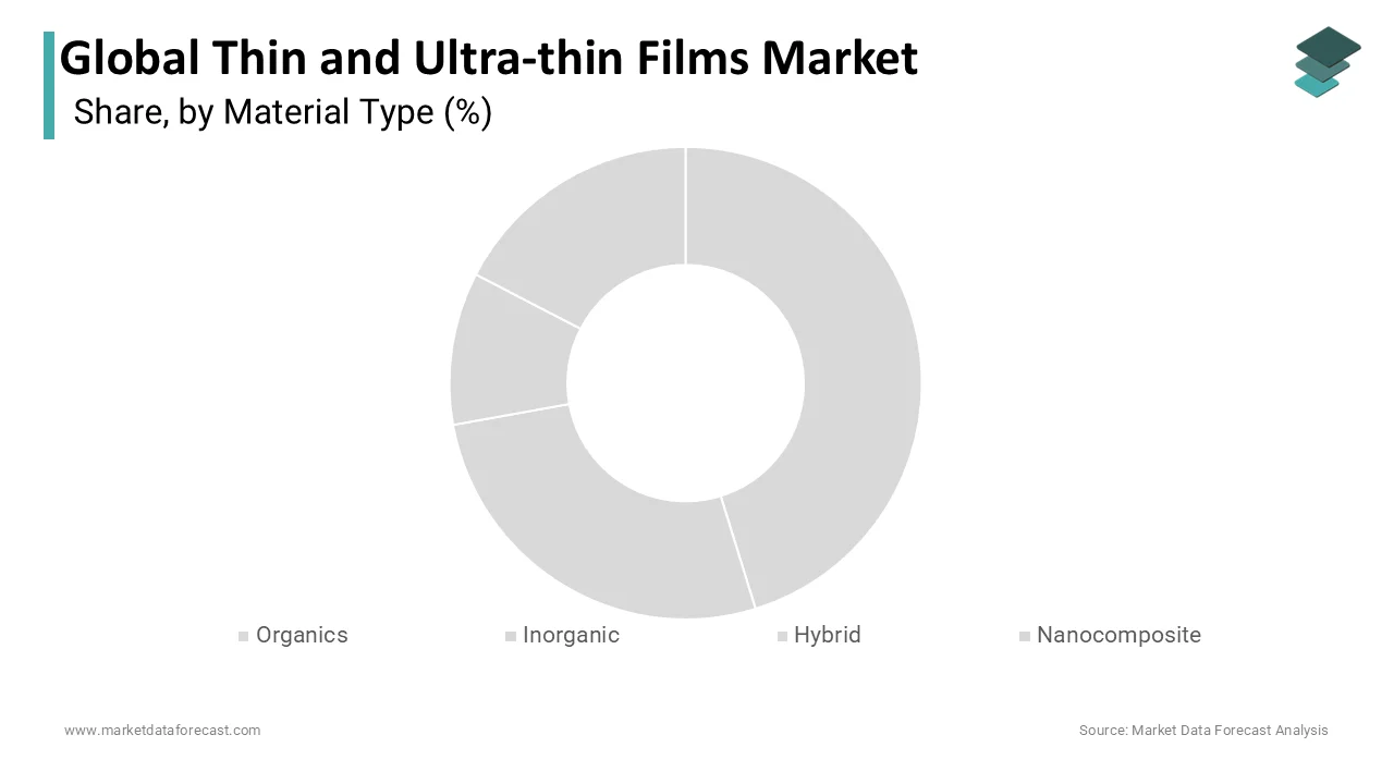
The nanocomposite thin films segment is likely to experience the fastest CAGR of 12.4% from 2025 to 2033. The rapid expansion of the nanocomposite thin films segment is driven by multifunctional performance in emerging applications. Nanocomposite films combining inorganic nanoparticles like alumina or silica within polymer matrices achieve water vapor transmission rates below 10 to the power of minus six grams per square meter per day, essential for organic light-emitting diode longevity. Foldable displays are incorporating advanced nanocomposite barriers designed to endure repeated folding cycles, according to sources. There is a growing emphasis in research and development on utilizing high-speed, continuous manufacturing methods for nanocomposite coatings, particularly for applications like flexible photovoltaics. This synergy of mechanical flexibility and hermetic sealing enables next-generation wearable and portable devices. Silver or zinc oxide nanoparticle-embedded nanocomposite films exhibit sustained antimicrobial activity critical for implantable devices. There is a noticeable increase in the use of sophisticated coating materials for medical applications. In addition, the number of newly cleared medical devices incorporating these advanced materials has expanded significantly. These newer devices include a range of products, such as catheters and orthopedic implants. A primary benefit of these composite coatings is their substantial effectiveness in minimizing surface bacterial adhesion. The substantial global volume of surgical implants, surpassing millions of units each year, is driving accelerated adoption of nanocomposites for their vital infection-resistant properties.
By Deposition Techniques Insights
The physical vapor deposition (PVD) segment held the largest share of 36.2% of the global thin and ultra-thin films market in 2025 due to its versatility, high deposition rates, and compatibility with metallic and ceramic coatings across industries. PVD is the standard method for depositing copper seed layers and tantalum nitride barriers in advanced interconnects. According to sources, copper damascene processes commonly utilize physical vapor deposition (PVD) for initial metal nucleation when manufacturing logic features under 20 nanometers. Modern logic fabrication of 300 millimeter wafers typically involves multiple PVD steps during the process. Apart from these, the consumption of tantalum for PVD targets remains consistent, reflecting ongoing demand from chip manufacturers. This entrenched role in high-volume semiconductor manufacturing secures PVD’s market dominance. Beyond electronics, PVD is widely used to apply wear-resistant titanium nitride and chromium nitride coatings on cutting tools, molds, and automotive trim. Carbide inserts are often supplied with a PVD-applied multi-layer coating. The use of such coatings can enhance the performance and longevity of tools. The adoption of PVD-coated tools has been increasing. This growth is associated with the demand for precision in various manufacturing applications. This dual use in high-tech and industrial sectors ensures broad and stable demand.
The atomic layer deposition (ALD) segment is on the rise and is expected to be the fastest-growing segment in the market by witnessing a CAGR of 14.1% during the forecast period. The swift growth of the ALD segment is attributed to its unmatched conformality and sub-angstrom thickness control. ALD is indispensable for depositing high-k gate oxides and capacitor dielectrics, where atomic-scale uniformity is non-negotiable. According to reports related to ALD technology in semiconductor manufacturing, there has been significant growth in the adoption and application of Atomic Layer Deposition tools in semiconductor fabrication facilities, reflecting a continuous industry trend of increasing reliance on this technology for advanced nodes. This precision makes ALD irreplaceable in Moore’s Law. ALD-deposited alumina and titania films provide pinhole-free moisture barriers for flexible OLEDs and implantable biosensors. As per sources, increasing stability of organic photodetectors, enabled by advanced encapsulation techniques like Atomic Layer Deposition (ALD), is a key trend in flexible electronics. According to studies, the field of implantable medical devices is seeing a general trend toward using highly conformal and hermetic ALD coatings to improve long-term biocompatibility and functionality. The rapid expansion of the flexible electronics and bioelectronics markets is fueling the exceptional growth of Atomic Layer Deposition (ALD), primarily due to ALD's unique capability to coat intricate 3D surfaces at low temperatures.
By End User Industry Insights
The semiconductor segment led the thin and ultra-thin films market and held a 42.5% share in 2025, as these films are fundamental to transistor architecture, interconnects packaging. Each new semiconductor node requires additional ultra-thin film layers to manage leakage current, electromigration, and heat dissipation. According to sources, the number of thin-film position steps required during the wafer fabrication process is generally increasing with each new technology generation. Gate oxides in modern transistors are becoming significantly thinner, now measuring only a few atomic layers thick. This relentless scaling makes film deposition not just a process step but a performance determinant. Fan-out wafer-level packaging and 3D stacking utilize ultra-thin dielectric and copper films for redistribution layers. Advanced packaging methods are becoming a more significant part of semiconductor manufacturing revenue. Specific types of thin-film processes represent the majority of associated capital investment within the assembly sector. One key integration platform uses copper pillars that are surrounded by barriers measuring less than 10 nanometers in thickness. This shift toward heterogeneous integration further entrenches semiconductor dominance.
The medical and biomedical applications segment is expected to exhibit a noteworthy CAGR of 13.8% from 2025 to 2033. The growth of the medical and biomedical applications segment is attributable to implantable electronics and diagnostic microdevices. Long-term implantable devices such as pacemakers, neural stimulators, and glucose monitors require ultra-thin hermetic coatings to prevent biofluid ingress. Advanced barrier technologies are being incorporated into implantable electronic devices. Thin film materials are demonstrating effectiveness in extending the functional lifespan of medical implants. Reliability requirements across medical technology are encouraging the use of robust protective coatings. Thin films of gold, titanium dioxide, or graphene oxide serve as transducer surfaces in point-of-care diagnostics. Multiple biosensor platforms utilize functionalized ultra-thin films for efficient antigen capture. Lateral flow assays incorporating nanostructured gold films have demonstrated high sensitivity for cardiac biomarkers during clinical validation. The expansion of decentralized diagnostics following the pandemic has heightened the demand for reproducible, high-surface-area transducer layers, thereby accelerating the integration of biomedical thin films.
REGIONAL ANALYSIS
Asia Pacific Thin And Ultra-Thin Films Market Analysis
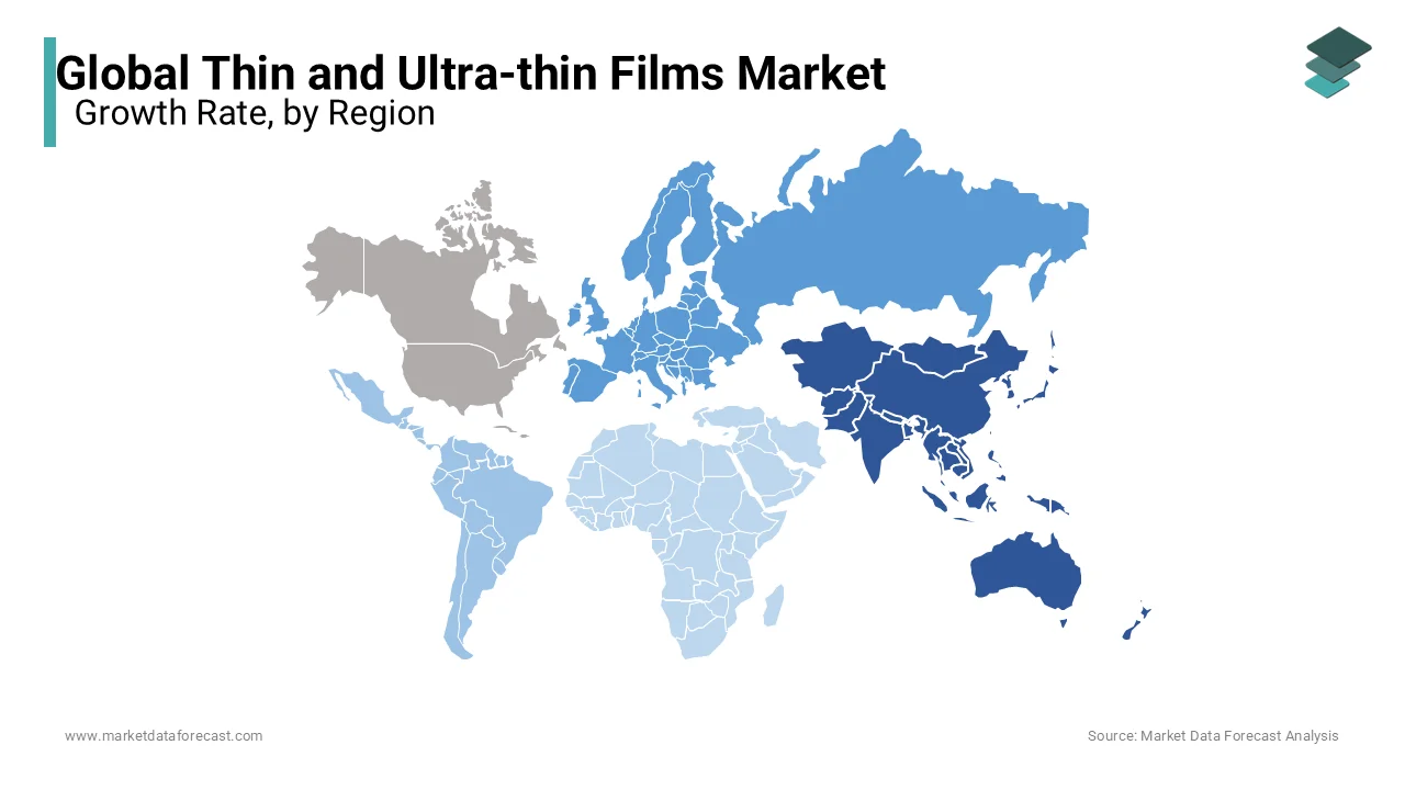
Asia Pacific was the top performer in the global thin and ultra-thin films market and accounted for a 45.5% share in 2025. The dominance of the APAC market is driven by semiconductor manufacturing concentration and consumer electronics assembly. South Korea stands as a regional powerhouse through Samsung and SK Hynix, which together account for a significant share of global DRAM production. There is a significant investment in increasing semiconductor capacity in some regions. Certain regions maintain a leading position in advanced chip manufacturing technologies, involving complex production steps per wafer. One country is pursuing an extensive strategy for developing its domestic chip manufacturing industry, which includes the construction of new production facilities. This push in domestic manufacturing is driving substantial consumption of key materials used in chip production. Another country is a key leader in supplying essential materials and equipment components for global chip manufacturing processes. This vertically integrated ecosystem, from materials to end devices, solidifies Asia Pacific’s unrivaled position.
North America Thin And Ultra-Thin Films Market Analysis
North America followed closely in the ultra-thin films market and held a 22.6% share in 2025 because of semiconductor design leadership and advanced R and D in quantum and photonic films. The United States is the central driver, with Intel, Micron, and Applied Materials anchoring domestic demand. Legislation has provided support for domestic semiconductor manufacturing, which has encouraged private investment. New facilities are under construction for advanced logic chip production in some regions. These new facilities are anticipated to require substantial quantities of specialized materials for production processes. Research in the field of renewable energy materials has resulted in advancements in solar cell efficiency. There is ongoing support for projects related to advanced optical coatings, which may have defense applications. This blend of commercial scale and frontier innovation sustains North America’s premium market role.
Europe Thin And Ultra-Thin Films Market Analysis
Europe secured a major region in the thin and ultra-thin films market due to materials science excellence and automotive electronics integration. Germany leads through equipment and specialty chemicals, with companies like Aixtron and Merck supplying CVD reactors and ALD precursors globally. Advanced lithography systems incorporate specialized multilayer mirrors. The mirrors feature numerous alternating ultra-thin films. Silicon photonics platforms utilize germanium films for high-speed data transmission components. The components are integrated into he data center infrastructure. Newer vehicles widely include thin-film-based sensors for advanced assistance systems and battery power management. Europe’s strength lies in high-precision niche applications rather than volume manufacturing.
Middle East and Africa Thin And Ultra-Thin Films Market Analysis
The Middle East and Africa region is an emerging player in the thin and ultra-thin films market, with growth centered on solar energy and defense modernization. Saudi Arabia is the regional leader through its Vision 2030 renewable energy targets. There is a trend toward adopting thin-film photovoltaics across energy initiatives. Cadmium telluride modules, specifically those utilizing ultra-thin absorber layers, are prominent in utility-scale installations. In aerospace, multi-layer ultra-thin optical coatings are employed on observation satellites to enhance spectral resolution capabilities. The defense sector is seeing investment in the development of ultra-thin radar-absorbing films designed for unmanned aerial vehicles. Efforts are underway to pilot the production of perovskite solar films aimed at expanding access to electricity in remote areas. While still nascent, this region’s strategic investments in energy and security create a distinct growth vector.
Latin America Thin And Ultra-Thin Films Market Analysis
Latin America is gradually expanding in the thin and ultra-thin films market from 2025 to 2033, with Brazil and Mexico driving demand through electronics assembly and scientific instrumentation. The use of aluminum and magnesium fluoride coatings for UV optics is a standard practice in space applications, often by NASA and ESA partners. Mexico is a growing hub in the global electronics supply chain, increasing its production of components, including sensors and displays. The mining industry, especially in major copper-producing nations like Chile, is exploring advanced sensor technologies for more efficient and real-time analysis of ore quality. Research institutions are developing advanced neutron detection techniques that utilize thin films, such as boron carbide layers, to improve efficiency and spatial resolution in various applications. Though small in scale, Latin America’s integration into North American supply chains and resource sector innovation ensures steady market expansion.
COMPETITIVE LANDSCAPE
The thin and ultra-thin films market features intense competition among vertically integrated equipment manufacturers, specialty chemical suppliers, nd materials innovators. Leadership is determined not by volume but by technological precision, process control, nd application expertise. Companies compete on film uniformity defect density and compatibility with next-generation device architectures rather than cost alone. The barrier to entry remains exceptionally high due to capital intensity, intellectual property density, nd stringent customer qualification protocols in the semiconductor and medical sectors. While North American and Japanese firms dominate equipment and precursor supply E,, European players excel in metrology and niche materials. Asian manufacturers are rapidly advancing through gogovernment-backednitiatives initiatives, but often rely on imported core technologies. Mergers and acquisitions target complementary deposition or metrology capabilities to offer integrated process solutions. Innovation cycles are accelerating as quantum photonics and bioelectronics demand films with aatomic-levelreproducibility creating a dynamic landscape where technical differentiation outweighs scale.
KEY MARKET PLAYERS
Companies playing a prominent role in the global thin and ultra-thin films market include
- Orange Thin Films (Netherlands)
- American Elements (US)
- ThinFilms Inc. (US)
- LEW TECHNIQUES LTD (UK)
- Angstrom Engineering Inc. (Canada)
- Denton Vacuum (US)
- Super Conductor Materials, Inc. (US)
- KANEKA CORPORATION (Japan)
- Arrow Thin Films, Inc. (US)
- Umicore (Belgium)
- Plasma-Therm (UK)
- Materion Corporation (US)
- INTEVAC, INC. (US)
- AIXTRON (Germany)
- GEOMATEC Co., Ltd. (Japan)
- Kurt J. Lesker Company (US)
- PVD Products, Inc. (US)
- Vital Materials Co., Limited (China)
- Praxair S.T. Technology, Inc. (US)
- AJA INTERNATIONAL, Inc. (US)
TOP LEADING PLAYERS IN THE MARKET
- Applied Materials Inc. is a global leader in materials engineering solutions with extensive capabilities in thin and ultra-thin film deposition technologies. The company supplies advanced physical vapor deposition, chemical vapor deposition, nd atomic layer deposition systems to semiconductor, display, and solar manufacturers worldwide. Its Endura and Centura platforms enable precise deposition of metallic dielectric and barrier films at the atomic scale, critical for sub-three-nanometer logic nodes. Applied Materials also expanded its Materials Engineering Technology Center in Singapore to accelerate co-development of novel film stacks for 3D NAND and GAA transistors, reinforcing its role as an innovation enabler in high-precision film manufacturing.
- Merck KGaA plays a pivotal role in the thin and ultra-thin films market through its Electron business unit, which supplies hhigh-purityprecursors photoresists, nd specialty materials for deposition and patterning. The company’s ALD and CVD precursors are essential for depositing hafnium oxide, aluminum oxide a,, nd metal nitride films in advanced semiconductor fabrication. The company also launched its Liqcreate portfolio of inorganic resist material, enabling sub-10-nanometer patterning. Collaborations with leading foundries on gate all around transistor integration further demonstrate Merck’s strategic alignment with next-generation device scaling and its commitment to enabling aatomic-levelfilm film control.
- ULVAC Inc. is a key Japanese manufacturer of vacuum equipment and thin film processing systems serving the semiconductor, flat panel display, nd photovoltaic industries. The company specializes in sputtering, evaporation, and plasma-enhanced chemical vapor deposition technologies for depositing conductive, electric, and optical films with nanometer precision. ULVAC’s multi-chamber tools support high-throughput production of transparent conductive oxides and barrier layers for flexible OLEDs. ULVAC also partnered with Japanese universities to develop low-temperature ALD processes for bioelectronic films. These initiatives underscore its focus on process innovation and expansion into emerging applications beyond traditional electronics manufacturing.
TOP STRATEGIES USED BY THE KEY MARKET PARTICIPANTS
Key players in the thin and ultra-thin films market prioritize vertical integration to secure high-purity raw materials and ensure supply chain resilience. They invest heavily in research and development to pioneer atomic-scale positioning techniques compatible with sub-three-nanometer semiconductor nodes. Strategic collaborations with semiconductor foundries and research institutions accelerate the development of aapplication-specificfilm film stacks. Geographic expansion into Asthe ia Pacific strengthens proximity to major electronics manufacturing hubs. Companies also focus on sustainability by developing low-energy deposition processes and recyclable target materials. Additionally, they enhance tool intelligence through embedded metrology and machine learning for real-time film thickness control. Diversification into emerging sectors such as quantum computing, flexible electronics, nd medical implants broadens revenue streams beyond traditional markets.
GLOBAL THIN AND ULTRA-THIN FILMS MARKET NEWS
- In May 2024, it was reported that the Fraunhofer Institute for Physical Measurement Techniques IPM, i collaboration with plasma system specialist Plasma Electronic GmbH, developed a Film-Inspect testing system. This is a new kind of sensor to check functional barrier layers on plastic or synthetic goods at the manufacturing pace. The sensor utilises infrared measurement technology to find thin coverings with a width of lower than 10 nm to 200 nm inline.
- In February 2024, experts at Osaka University made an innovative flexible optical sensor that functions even when wrinkled. It is a soft, malleable, nd wireless optical sensor employing natural transistors and carbon nanotubes on an ultra-thin polymer film. This development is believed to present new avenues in imaging technologies and non-destructive analysis methods.
MARKET SEGMENTATION
This research report on the global thin and ultra-thin films market has been segmented and sub-segmented based on material type, deposition techniques, end-user industry, and region.
By Material Type
- Organics
- Inorganic
- Hybrid
- Nanocomposite
By Deposition Techniques
- Physical Vapor Deposition (PVD)
- Chemical Vapor Deposition (CVD)
- Spray Pyrolysis
- Atomic Layer Deposition (ALD)
- Sol-Gel Processing
By End-User Industry
- Electronic
- Semiconductor
- Energy and Power Generation
- Healthcare, Medica, and Biomedical Applications
- Automotive and Transportation
- Defence and Aerospace
- Others
By Region
- North America
- Europe
- Asia Pacific
- Latin America
- Middle East & Africa