Global Advanced Packaging Market Size, Share, Trends, and Growth Analysis Report, Segmented By Packaging Platform, End-User Industry, Device Architecture, Interconnect Technology, & Region (North America, Europe, Latin America, Asia Pacific, Middle East & Africa), Industry Forecast From 2026 to 2034
Global Advanced Packaging Market Size
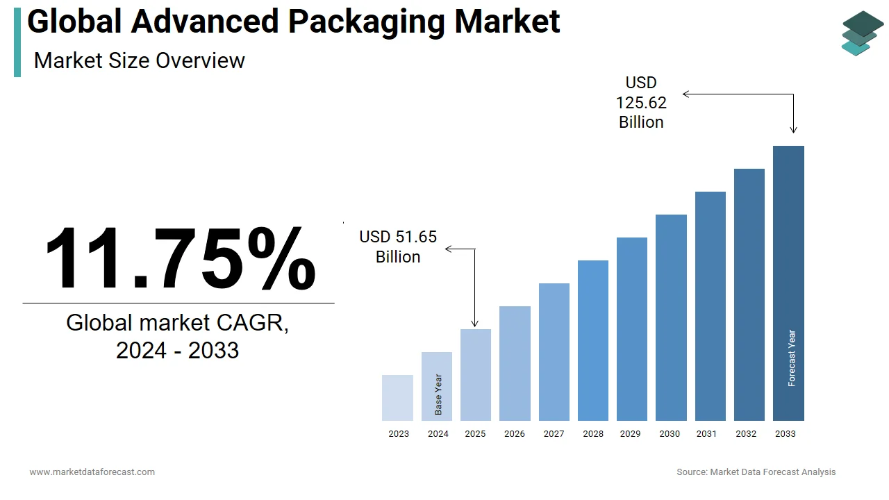
The size of the global advanced packaging market was worth USD 51.65 billion in 2025. The global market is anticipated to grow at a CAGR of 11.75% from 2026 to 2034 and be worth USD 140.38 billion by 2034 from USD 57.72 billion in 2026.
The advanced packaging is an innovative semiconductor packaging technology designed to enhance the performance, density, and reliability of electronic devices. According to IC Insights, over 70% of modern high-performance chips employ some form of advanced packaging to meet escalating consumer and industrial demands. The surge in applications such as AI accelerators, 5G devices, and high-end computing systems is driving adoption.
MARKET DRIVERS
Rising Demand for High-Performance Computing Devices
The proliferation of AI, machine learning, and cloud computing requires semiconductor devices with higher processing capabilities and faster interconnects is fuelling the growth of the advanced packaging market. Advanced packaging technologies, such as 2.5D and 3D ICs, enable improved signal integrity and reduced latency. According to Gartner, data center processor shipments grew 12% in 2023, reflecting the need for high-performance chips. The demand for energy-efficient, compact devices in HPC, gaming, and consumer electronics is propelling the adoption of advanced packaging solutions.
Miniaturization and Space Efficiency in Electronics
Consumer demand for smaller, lighter, and multifunctional devices is intensifying the need for space-efficient packaging. Advanced packaging techniques, including fan-out wafer-level packaging (FOWLP), reduce package size while maintaining or improving performance. As per Yole Développement, smartphone production exceeded 1.4 billion units in 2023, with increasingly thinner form factors requiring compact semiconductor solutions.
MARKET RESTRAINTS
High Manufacturing Costs
Advanced packaging processes require specialized equipment, cleanroom facilities, and precise alignment techniques, which is leading to elevated manufacturing costs. These high costs limit adoption among mid-sized electronics manufacturers and increase overall product prices. The complexity of handling thin wafers, multiple dies, and advanced interposers adds operational challenges, which constrain broader implementation in cost-sensitive markets like consumer electronics.
Supply Chain Constraints and Material Limitations
Advanced packaging relies on specialized substrates, underfill materials, and solder interconnects, which face periodic supply shortages. Material constraints can lead to delays and reduced throughput for high-volume manufacturers. Additionally, sourcing advanced packaging materials that meet thermal, electrical, and mechanical requirements while remaining cost-effective presents a persistent challenge in emerging markets where supply chain infrastructure is less mature.
MARKET OPPORTUNITIES
Integration with AI and 5G Technologies
The rollout of 5G networks and AI applications is creating new opportunities for the growth of the advanced packaging market. High-speed signal transmission and dense interconnects are next-generation processors and baseband chips. As per Ericsson, global 5G subscriptions surpassed 1.1 billion in 2023, driving demand for high-performance chips packaged using advanced techniques. Integrating multiple dies within a single package for AI accelerators or 5G RF modules offers manufacturers efficiency and performance gains, which are creating lucrative business opportunities for packaging solution providers.
Expansion in Automotive Electronics
Automotive electrification and autonomous vehicle technologies are increasing the requirement for high-performance, miniaturized semiconductor devices, which additionally fuels the growth of the advanced packaging market. According to McKinsey, the average electric vehicle contains 2,000–3,000 semiconductor components, many of which demand advanced packaging for thermal and reliability management. Advanced packaging allows integration of power ICs, sensors, and processors in compact modules by enabling safer and more efficient vehicle electronics. The automotive sector’s ongoing shift toward electric and connected vehicles represents a growing and stable market for advanced packaging providers.
MARKET CHALLENGES
Technical Complexity and Skill Shortages
Advanced packaging processes demand highly skilled personnel, and sophisticated process control is one of the challenging factors for the growth of the advanced packaging market. As per IPC, the semiconductor industry faces a 15% shortage in specialized packaging engineers globally. The complexity of 3D stacking, interposer alignment, and heterogeneous integration increases defect risks, resulting in lower yields and higher production costs. This technical barrier hinders smaller players from entering the market and slows widespread adoption of innovative packaging techniques.
Rapid Technological Obsolescence
The pace of semiconductor innovation is accelerating, requiring continuous R&D investment. Technologies like chiplets, FOWLP, and 3D ICs evolve quickly, rendering older packaging solutions obsolete within a few years. As per IC Insights, lifecycle turnover for advanced packaging technologies has decreased from seven years to under four years. Manufacturers must constantly innovate to remain competitive, which presents a significant challenge in capital allocation, risk management, and maintaining supply chain readiness.
REPORT COVERAGE
| REPORT METRIC | DETAILS |
| Market Size Available | 2025 to 2034 |
| Base Year | 2025 |
| Forecast Period | 2026 to 2034 |
| Segments Covered | By Packaging Platform, End-User Industry, Device Architecture, Interconnect Technology, and Region. |
| Various Analyses Covered | Global, Regional and Country-Level Analysis, Segment-Level Analysis, Drivers, Restraints, Opportunities, Challenges; PESTLE Analysis; Porter’s Five Forces Analysis, Competitive Landscape, Analyst Overview of Investment Opportunities |
| Regions Covered | North America, Europe, APAC, Latin America, Middle East & Africa |
| Market Leaders Profiled | Amkor Technology, Inc., Taiwan Semiconductor Manufacturing Company Limited, Advanced Semiconductor Engineering Inc., Intel Corporation, JCET Group Co. Ltd. |
SEGMENTAL ANALYSIS
By Packaging Platform Insights
The flip-chip technology segment was the largest and held 48.2% of the advanced packaging market share in 2024 with its superior electrical performance, miniaturization capability, and thermal efficiency. According to Yole Développement, flip-chip accounted for approximately 48% of global advanced packaging shipments in 2023. One key driver is the demand for high-density interconnects in smartphones, tablets, and high-performance computing devices. Flip-chip enables reduced signal path lengths and better heat dissipation, which is for AI accelerators and graphics processors.
The Fan-in WLP segment is augmented to grow with an expected CAGR of 13.5% during the forecast period, with its compact form factor, cost-efficiency, and suitability for consumer electronics. As per SEMI, smartphone penetration exceeded 1.4 billion units globally in 2023, which is pushing demand for space-efficient packaging solutions. FOWLP reduces package size while maintaining electrical performance, making it ideal for wearable devices, IoT sensors, and mobile chips. Additionally, the integration of multiple dies in FOWLP packages supports high-density interconnects by enhancing the performance of multifunctional devices without increasing overall footprint.
By End-User Industry Insights
The consumer electronics segment held 52.3% of the advanced packaging market share in 2024, with the rising smartphone, tablet, and wearable device sales driving the demand for advanced packaging solutions. According to IDC, global smartphone shipments exceeded 1.4 billion units in 2023, while wearable device adoption increased by 19%. Advanced packaging technologies, including flip-chip and FOWLP, allow manufacturers to integrate multiple functionalities into compact packages, supporting high-speed processing and energy efficiency.
The data center and HPC segment is likely to grow with an expected CAGR of 14.2% during the forecast period due to rising AI workloads, cloud computing, and server performance requirements. Advanced packaging, such as 2.5D and 3D ICs, facilitates high interconnect density and superior thermal management, crucial for multi-die server processors and AI accelerators. The adoption of these solutions enhances performance, reliability, and energy efficiency in data centers, which is driving faster growth compared to other sectors.
By Interconnect Technology Insights
The solder bump technology segment was the largest and held 55.3% of the advanced packaging market share in 2024 with its proven reliability, ease of implementation, and compatibility with flip-chip and wafer-level packaging. According to TechInsights, over 70% of high-performance ICs utilize solder bumps for electrical interconnects. Solder bumps ensure high conductivity and robust mechanical bonding between die and substrate for smartphones, GPUs, and server-grade processors. Their cost-effectiveness relative to copper pillar and hybrid bonding also reinforces market preference.
The hybrid bonding segment is projected to grow at a CAGR of 15% from 2025 to 2033 due to its ability to achieve ultra-high-density interconnects and superior performance for AI and HPC applications. As per SEMI, the adoption of hybrid bonding in 3D ICs grew by 22% in 2023. The technology enables both electrical and mechanical connections at the micro-scale, reducing interconnect length, improving signal integrity, and supporting smaller die sizes. The growing demand for heterogeneous integration in next-gen semiconductors makes hybrid bonding the fastest-growing interconnect segment.
REGIONAL ANALYSIS
Asia Pacific Advanced Packaging Market Analysis
Asia Pacific dominated the advanced packaging market with a 45.3% share due to extensive semiconductor manufacturing infrastructure in Taiwan, South Korea, and China. According to IC Insights, over 60% of global semiconductor assembly and packaging occurs in this region. High consumer electronics production and rapid adoption of AI, IoT, and 5G devices drive regional growth. Leading foundries and OSATs (outsourced semiconductor assembly and test providers) in APAC continue to expand advanced packaging capabilities to meet increasing demand.
North America Advanced Packaging Market Analysis
North America advanced packaging market growth is likely to grow with the semiconductor design hubs in the U.S. and high demand for HPC and AI solutions. According to Gartner, AI chip adoption in North America grew 18% in 2023. Advanced packaging supports the integration of heterogeneous dies and enhances system performance in data centers and automotive electronics. Investments in domestic packaging facilities aim to reduce dependency on overseas manufacturing.
Europe Advanced Packaging Market Analysis
Europe advanced packaging market growth is likely to grow, supported by automotive electronics, industrial automation, and aerospace applications. According to McKinsey, the European EV market grew by 20% in 2023, necessitating high-performance semiconductor packages. European players focus on integrating advanced packaging solutions into automotive and industrial semiconductors to meet stringent reliability and thermal requirements.
Latin America Advanced Packaging Market Analysis
Latin America advanced packaging market growth is driven by increased adoption of consumer electronics and industrial automation. As per IDC, smartphone and wearable device shipments grew 15% in 2023. Regional adoption of advanced packaging is increasing gradually due to emerging manufacturing hubs and growing local electronics consumption.
Middle East & Africa Advanced Packaging Market Analysis
The advanced packaging market growth is likely to be driven by government-backed technology initiatives and smart infrastructure projects. According to World Bank data, Middle East investment in electronics and industrial automation increased by 10% in 2023. The focus on developing domestic semiconductor capabilities and smart city projects is gradually supporting advanced packaging adoption.
COMPETITIVE LANDSCAPE
The Advanced Packaging Market is highly competitive, driven by rapid technological innovation and rising demand in APAC, North America, and Europe. ASE, Amkor, and JCET dominate through extensive regional operations, R&D investments, and strategic alliances. Companies compete on technological capabilities, production efficiency, and the ability to provide end-to-end packaging solutions. In APAC, rapid smartphone adoption, AI chip proliferation, and automotive electronics growth have intensified the competition. Continuous advancements in flip-chip, fan-out WLP, and hybrid bonding solutions serve as key differentiators. Market players focus on shortening product cycles and offering high-density integration to capture clients requiring miniaturized and high-performance semiconductor solutions.
KEY MARKET PLAYERS
Some of the companies that are playing a dominating role in the global advanced packaging market include
- Amkor Technology, Inc.
- Taiwan Semiconductor Manufacturing Company Limited
- Advanced Semiconductor Engineering Inc.
- Intel Corporation
- JCET Group Co. Ltd
Top Players in the Advanced Packaging Market
- ASE Technology, headquartered in Taiwan, is a leading provider of semiconductor assembly and testing services with a strong presence in the Asia Pacific region. The company has been instrumental in advancing 2.5D and 3D packaging technologies, supporting high-performance computing and mobile applications. ASE invests heavily in research and development to enhance heterogeneous integration and fan-out wafer-level packaging. Recent initiatives include expanding production facilities in Taiwan and China to meet growing demand for high-density interconnects. ASE’s collaborations with global semiconductor designers have strengthened its position as a key enabler of next-generation electronic devices.
- Amkor, a U.S.-based semiconductor packaging and test provider, has a significant footprint in the Asia Pacific market, particularly in China, South Korea, and Malaysia. The company specializes in flip-chip, wafer-level, and advanced system-in-package (SiP) solutions. Amkor continuously invests in production technology upgrades and capacity expansion to address rising demand from consumer electronics, automotive, and data center segments. The company also engages in strategic partnerships with leading semiconductor designers in APAC to deliver customized packaging solutions and improve supply chain efficiency by enhancing its regional market dominance.
- JCET, headquartered in China, is a major player in semiconductor advanced packaging and testing services across the Asia Pacific. The company focuses on fan-in/fan-out WLP, flip-chip, and 3D IC technologies to support AI, automotive, and consumer electronics applications. JCET has expanded its manufacturing footprint in China and Southeast Asia, enhancing its capacity to serve high-demand markets. Collaborations with global chip designers and investment in R&D for heterogeneous integration and miniaturized packages have reinforced JCET’s market position, which is making it a preferred partner for regional semiconductor assembly and advanced packaging solutions.
MARKET SEGMENTATION
This research report on the global advanced packaging market has been segmented and sub-segmented into the following categories.
By Packaging Platform
- Flip-Chip
- Embedded Die
- Fan-in WLP
- Fan-out WLP
- 5D / 3D
By End-User Industry
- Consumer Electronics
- Automotive and EV
- Data Center and HPC
- Industrial and IoT
- Healthcare / Med-tech
By Device Architecture
- 2D IC
- 2.5D Interposer
- 3D IC (TSV / Hybrid-Bond)
By Interconnect Technology
- Solder Bump
- Copper Pillar
- Hybrid Bond
By Region
- North America
- Europe
- Asia Pacific
- Latin America
- The Middle East and Africa
Frequently Asked Questions
1. What is the Advanced Packaging Market?
The Advanced Packaging Market involves innovative semiconductor packaging technologies that enable higher integration, performance, compactness, and reliability of chips for AI, automotive, consumer electronics, and telecom applications
2. What are key packaging types in the Advanced Packaging Market?
Flip-chip, fan-out wafer-level, embedded-die, fan-in wafer-level, 2.5D/3D packaging, and system-in-package are major types, with flip-chip and 2.5D/3D posting the fastest growth
3. Which industry verticals drive demand in the Advanced Packaging Market?
Consumer electronics, automotive electronics, telecommunications (5G, IoT), healthcare, and industrial automation are the largest end-user segments globally
4. Why is Asia Pacific dominant in the Advanced Packaging Market?
Asia Pacific leads, with over 43–65% market share in 2024–2025, supported by investments in semiconductor manufacturing in China, Taiwan, South Korea, and India
5. What main trends shape the Advanced Packaging Market?
Heterogeneous integration, miniaturization, advanced thermal and signal management, sustainable packaging practices, and government subsidies for semiconductor R&D are key trends
6. Who are the top companies in the Advanced Packaging Market?
ASE, Amkor Technology, TSMC, Samsung Electronics, Texas Instruments, Brewer Science, SUSS MicroTec, ChipMOS, and Powertech Technology are major players
7. How do automotive applications influence the Advanced Packaging Market?
EVs and autonomous driving push demand for high-reliability, compact power electronics and domain controllers, resulting in over 12.4% CAGR for automotive/EV packaging
8. What is hybrid bonding in the Advanced Packaging Market?
Hybrid bonding is a metal-to-metal link below 10 μm pitch, vital for bandwidth and thermal performance, with fastest growth among interconnect technologies
9. How does AI and HPC impact the Advanced Packaging Market?
AI and high-performance computing require advanced integration, increased density, and improved thermal reliability—the market is directly shaped by these trends
10. What challenges exist in the Advanced Packaging Market?
High capital intensity, substrate shortages (such as BT-resin), supply chain volatility, and material costs can constrain near-term growth
Related Reports
Access the study in MULTIPLE FORMATS
Purchase options starting from
$ 2500
Didn’t find what you’re looking for?
TALK TO OUR ANALYST TEAM
Need something within your budget?
NO WORRIES! WE GOT YOU COVERED!
Call us on: +1 888 702 9696 (U.S Toll Free)
Write to us: sales@marketdataforecast.com