Europe Advanced Packaging Market Size, Share, Trends, and Growth Analysis Report, Segmented By Type, End User, and Country – Industry Forecast From 2026 to 2034
Market Size, 2025
$9.73 BnMarket Estimate, 2026
$10.54 BnMarket Forecast, 2034
$20.04 BnCAGR, 2026–2034
8.36%Europe Advanced Packaging Market Report Summary
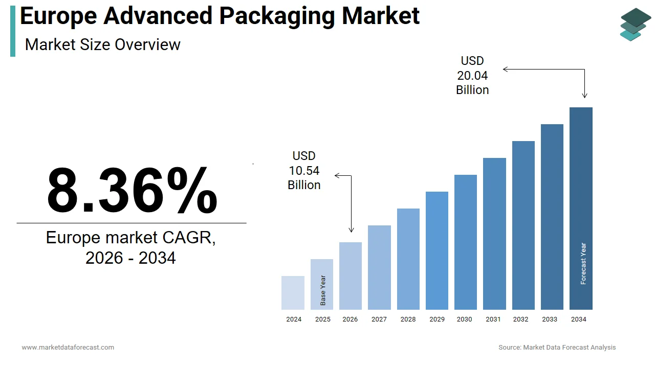
The Europe advanced packaging market was valued at USD 9.73 billion in 2025, is estimated to reach USD 10.54 billion in 2026, and is projected to reach USD 20.04 billion by 2034, growing at a CAGR of 8.36% from 2026 to 2034. The growth of the market is driven by Europe’s strategic push for semiconductor sovereignty under the EU Chips Act, rising demand for energy-efficient electronics, and expanding applications in automotive, AI, 5G, and high-performance computing. Advanced packaging technologies such as flip chip, fan-out wafer-level packaging, and 2.5D/3D integration are enabling higher performance, improved thermal management, and greater integration density. The region’s emphasis on sustainable electronics, circular economy practices, and supply chain resilience is further shaping the evolution of advanced packaging across Europe.
Key Market Trends
- Strong policy support for semiconductor sovereignty under the EU Chips Act.
- Rising adoption of energy-efficient packaging solutions in electric vehicles and data centers.
- Increasing use of heterogeneous integration for AI and edge computing hardware.
- Growing demand for ruggedized packaging in aerospace and defense electronics.
- Rising focus on sustainable and recyclable packaging materials to meet environmental regulations.
Segmental Insights
- Based on type, the Flip Chip Ball Grid Array (FCBGA) segment dominated the Europe advanced packaging market by capturing 32.4% share in 2024. This dominance is driven by its superior electrical performance, high interconnect density, and excellent thermal management for high-power applications such as AI processors, data center CPUs, and automotive domain controllers. FCBGA remains the preferred solution for advanced driver assistance systems and battery management units in electric vehicles.
- Based on end user, the automotive segment led the market with 38.2% share in 2024, supported by Europe’s leadership in premium vehicle manufacturing and strict regulatory requirements for electrification and safety systems. Advanced packaging is critical for EV inverters, battery management, and autonomous driving platforms that require high reliability and thermal stability.
Regional Insights
The Europe advanced packaging market is witnessing steady growth across major economies, supported by strong industrial demand, public investment, and technological leadership in semiconductor manufacturing.
- Germany was the largest contributor, accounting for 24.1% market share in 2024, driven by Infineon’s advanced packaging facilities, a strong automotive sector, and government-backed semiconductor initiatives.
- France ranked second with 18.7% share, supported by its national semiconductor strategy, aerospace and defense leadership, and integrated packaging capabilities at STMicroelectronics’ Crolles site.
Competitive Landscape
The Europe advanced packaging market is characterized by a concentrated and highly specialized competitive environment dominated by integrated device manufacturers. Unlike Asia’s high-volume outsourced packaging model, Europe’s ecosystem focuses on in-house, high-reliability solutions for automotive, industrial, and defense applications. Competition is driven by thermal performance, signal integrity, sustainability, and co-design capabilities rather than price. Public-private partnerships, EU-funded pilot lines, and research collaborations with institutes such as imec, CEA Leti, and Fraunhofer play a critical role in sustaining innovation. Companies that align technological leadership with EU policy goals and end-user requirements are best positioned to lead Europe’s advanced packaging landscape.
Prominent companies in the Europe advanced packaging market include Qualcomm Incorporated, Intel Corporation, IBM Corporation, Texas Instruments, Inc., Analog Devices, Inc., Microchip Technology Incorporated, NXP Semiconductors, Infineon Technologies AG, STMicroelectronics, Samsung Electronics Co., Ltd., Renesas Electronics Corporation, and VMware, Inc. (Broadcom Inc.).
Europe Advanced Packaging Market Size
The size of the Europe advanced packaging market was worth USD 9.73 billion in 2025. The regional market is anticipated to grow at a CAGR of 8.36% from 2026 to 2034 and be worth USD 20.04 billion by 2034 from USD 10.54 billion in 2026.
Advanced packaging refers to highly engineered semiconductor packaging technologies that enhance performance, power efficiency, and integration density beyond traditional wire-bonded packages. These include flip chip wafer level packaging, 25D and 3D integration, fan out wafer level packaging, and system in package solutions. This segment is important for enabling next-generation applications in artificial intelligence, high-performance computing, automotive electronics, and 5G infrastructure. The European Commission is actively evaluating the progress of the Chips Act, with a key focus on expanding the region’s capacity for advanced semiconductor packaging and manufacturing to enhance industrial sovereignty. The continent’s strategic emphasis on semiconductor sovereignty has intensified focus on packaging as a key node in the supply chain. European entities continue to display strong inventive activity in electronics and microsystems, contributing significantly to the global patent landscape, particularly in electrical machinery and computer technology. The accelerating generation of electronic waste in Europe highlights a critical, growing need for sustainable, eco-friendly packaging solutions that facilitate easier disassembly and the recovery of valuable materials. These intersecting imperatives, technological advancement, strategic autonomy, and circularity, define the evolving landscape of advanced packaging in Europe.
MARKET DRIVERS
Europe’s Strategic Push for Semiconductor Sovereignty Under the EU Chips Act
The European Union’s Chips Act represents a foundational driver for Europe advanced packaging market. It achieves this by embedding packaging capability within its vision of resilient domestic semiconductor supply chains. The European Commission is mobilizing significant public and private investment through the European Chips Act to strengthen semiconductor manufacturing capacity and secure the supply chain by 2030, with a strong focus on fostering advanced packaging and testing capabilities within the EU. This initiative responds to Europe’s current dependency. The European Union currently holds a small percentage of global semiconductor production capacity compared to its consumption, prompting the European Chips Act to aim for a significant increase in its global market share to reduce dependency on foreign suppliers. Crucially, the Act identifies advanced packaging as a near term opportunity where Europe can regain leadership without requiring the extreme cleanroom infrastructure of leading-edge fabrication. STMicroelectronics in France and Infineon in Germany have already committed to building advanced packaging lines for automotive and power electronics. The European Processor Initiative is working to develop a family of low-power processors to improve European supercomputing capabilities, aiming to build a sovereign, sustainable, and secure ecosystem. This policy-induced vertical integration ensures sustained demand for advanced packaging services within the region, fostering ecosystem development from materials suppliers to equipment vendors.
Rising Demand for Energy-Efficient Electronics in Automotive and Data Infrastructure
The deployment of electric vehicles and energy-conscious data centers is accelerating the expansion of the Europe advanced packaging market. This is due to the technology's inherent thermal and electrical advantages. Data centers in Europe are experiencing high growth in electricity demand, with energy usage approaching levels comparable to the residential consumption of major European nations. Moreover, data centers are actively addressing energy losses by optimizing cooling and power delivery systems to combat the rise in power density. Advanced chip packaging techniques are accelerating efficiency improvements in server CPUs by shortening interconnects and reducing power waste. The rapid shift to electric vehicles and advanced, sensor-heavy driving systems has drastically increased the number of semiconductors required per vehicle. In addition, the adoption of advanced, embedded packaging for power semiconductors in electric vehicle inverters is enabling significant reductions in physical size while improving heat dissipation. Stricter EU energy labeling and CO2 fleet targets have elevated these packaging innovations from optional enhancements to critical compliance enablers.
MARKET RESTRAINTS
High Capital Intensity and Limited Access to Specialized Packaging Equipment
The extraordinary capital cost and supply barrier for specialized equipment constrain the growth of the Europe advanced packaging market. Advanced packaging lines require precision tools for hybrid bonding, wafer thinning, and heterogeneous integration, with single tools costing a significant amount. European specialized packaging firms are facing extended lead times due to surging global demand from Asian markets for advanced semiconductor packaging technology. This scarcity forces European foundries to prioritize high-volume consumer chip packaging over specialized automotive or industrial applications. Moreover, European semiconductor startups are facing significant scaling barriers due to high capital requirements and competition for advanced equipment access, necessitating greater financial and strategic support. National subsidies often cover only a portion of tool costs, leaving a financing gap that deters new entrants. Europe's lack of coordinated procurement and shared fabrication for next-gen packaging (chiplets, silicon interposers) threatens to leave it behind its global rivals, undermining its leading design strengths.
Stringent Environmental Regulations on Hazardous Materials and Waste Handling
The region’s progressive environmental legislation imposes complex restraints on advanced packaging processes. This hampers the expansion of the Europe advanced processing market. These processes rely on lead-based solders, brominated flame retardants, and perfluorinated compounds. Proposed regulatory updates concerning material restrictions for semiconductor packaging components may require alterations in existing assembly workflows. Adjusting to these material modifications entails the reformulation of materials and a re-evaluation of assembly processes. The re-evaluation of assembly methods for advanced packages is frequently a resource-intensive and lengthy process. Rules governing the recovery of electronics are promoting enhancements in the recyclability of intricate, multi-layered, or encapsulated packaging structures. Some advanced packaging configurations, such as those with embedded parts, might encounter difficulties in achieving specific recyclability goals. These regulatory pressures compel packaging developers to balance performance with circularity, a dual objective that slows innovation cycles and increases time to market compared to less regulated regions.
MARKET OPPORTUNITIES
Integration of Advanced Packaging in European Defense and Aerospace Electronics
The region’s defense sector offers a potential opportunity for advanced packaging through demand for ruggedized high-reliability electronic systems, which is expected to boost the growth of the Europe advanced packaging market. There is an increased demand for electronic packaging capable of enduring extreme thermal conditions and radiation due to commitments to enhance command and control infrastructure. The expense and significant mass of conventional ceramic housings are driving the development of more efficient molded and embedded options. Satellite navigation programs are more frequently adopting wafer-level packaging to reduce signal processor weight while maintaining dependable communication. Contemporary fighter jet initiatives are incorporating multi-dimensional stacked packaging to optimize computing power within limited spaces. Environmental sustainability efforts now prioritize the design of electronics packaging intended to support safe disintegration at the end of a hardware cycle. These mission-critical applications offer premium margins and long-term contracts, enabling European packaging specialists to offset R&D costs and scale capabilities for commercial markets.
Growth of Heterogeneous Integration for AI and Edge Computing Hardware
The proliferation of artificial intelligence at the network edge is creating demand for heterogeneous integration where advanced packaging combines logic, memory, and sensors into single modules, which provides fresh prospects for the European advanced processing market. A significant portion of European research initiatives focused on artificial intelligence now necessitates specialized advanced packaging techniques. Integrating components in a two-and-a-half-dimensional arrangement has shown potential for substantial increases in memory bandwidth. These systems cannot rely on standard packages due to data bottleneck constraints. Many new advanced driver-assistance system platforms are incorporating system-in-package solutions to enhance performance. Automotive edge AI is equally influential. System-in-package configurations for automotive assistance systems often position processors and memory in proximity to one another. This architectural shift transforms packaging from a back-end process to a co-design enabler. These integrated packages turn packaging into a compliance instrument and a performance booster, allowing for hardware-level monitoring of model behavior to meet EU AI Act mandates for efficiency and transparency.
MARKET CHALLENGES
Fragmentation of the European Semiconductor Packaging Ecosystem
The lack of vertical integration across the region’s semiconductor packaging value chain hinders the growth of the Europe advanced processing market. Unlike Asia, where foundries, packaging houses, and equipment makers operate in coordinated clusters, European players are geographically and functionally dispersed. Major European semiconductor hubs, particularly in Germany and France, are actively integrating wafer fabrication and advanced packaging to secure supply chains, supported by the broader EU-driven coalition to enhance regional manufacturing sovereignty. This fragmentation increases logistics complexity and intellectual property leakage risks. For example, a chip designed in Sweden may be fabricated in Italy, packaged in the Netherlands, and tested in Ireland, adding several weeks to the time to market, as per research. Moreover, standardization gaps persist. German automotive manufacturers mandate that complex electronic modules for vehicles meet stringent, standardized reliability and stress-test certifications to comply with industry quality demands. The absence of a harmonized EU packaging strategy and collaborative pilot facilities hinders the ability of startups and SMEs to scale up their prototyping efforts. This disunity undermines the EU’s ambition to become a self-reliant semiconductor region despite strong individual capabilities in design and materials.
Shortage of Skilled Workforce in Advanced Packaging Engineering
The region faces a major talent gap in process integration, yield analysis, and materials science specific to advanced packaging. Consequently, this inhibits the expansion of the Europe advanced processing market. The semiconductor sector faces a substantial need for additional personnel, with a noted difficulty in filling advanced packaging positions. This challenge in hiring for specialized roles may be linked to academic programs that are not current with industry demands. Managers in the packaging field indicate trouble finding engineers with expertise in advanced methods like hybrid bonding or thermal simulation. Universities rarely offer dedicated courses in 3D integration or fan-out packaging, preferring traditional electronics tracks. The result is a reliance on expatriate talent. This dependency creates vulnerability to immigration policy shifts and knowledge transfer barriers. Even vocational programs lag. Packaging innovation in Europe is currently restricted more by skill shortages than by technology; this will continue until the educational pipeline is aligned with industry demands.
REPORT COVERAGE
| REPORT METRIC | DETAILS |
| Market Size Available | 2025 to 2034 |
| Base Year | 2025 |
| Forecast Period | 2026 to 2034 |
| Segments Covered | By Type, End User, and Country. |
| Various Analyses Covered | Global, Regional, and Country-Level Analysis, Segment-Level Analysis, Drivers, Restraints, Opportunities, Challenges; PESTLE Analysis; Porter’s Five Forces Analysis, Competitive Landscape, Analyst Overview of Investment Opportunities |
| Countries Covered | UK, France, Spain, Germany, Italy, Russia, Sweden, Denmark, Switzerland, Netherlands, Turkey, Czech Republic, and the Rest of Europe. |
| Market Leaders Profiled | Qualcomm Incorporated (Qualcomm Technologies, Inc.), Intel Corporation, IBM Corporation, Texas Instruments, Inc., Analog Devices, Inc., Microchip Technology Incorporated, NXP Semiconductors, Infineon Technologies AG, STMicroelectronics, Samsung Electronics Co., Ltd. (Samsung Group), Renesas Electronics Corporation, VMware, Inc. (Broadcom Inc.), and Others. |
SEGMENTAL ANALYSIS
By Type Insights
The Flip Chip Ball Grid Array (FCBGA) segment dominated the Europe advanced packaging market by accounting for a 32.4% share in 2024. The dominance of the FCBGA is driven by its superior electrical performance, thermal management, and scalability for high pin count applications prevalent in data infrastructure and automotive computing. FCBGA is the de facto standard for packaging high core count processors used in artificial intelligence and cloud computing due to its low inductance and high interconnect density. These systems require sustained thermal performance under 250-watt loads, a threshold where FCBGA’s integrated heat spreader and direct flip chip attach outperform wire-bonded alternatives. The energy efficiency imperative further reinforces this choice. Modern vehicles increasingly rely on centralized domain controllers that demand high reliability and thermal stability, qualities inherent to FCBGA. The majority of newly launched electric vehicle platforms in Europe utilize FCBGA packaged systems on chip, particularly for advanced driver assistance and battery management applications. High-performance automotive microcontrollers, such as the AURIX TC4x family, are increasingly designed with FCBGA to manage high processing demands while maintaining strict junction temperatures for safety qualification. The implementation of updated European safety regulations, which requireadvanced emergency braking and lane-keeping systems, is accelerating the adoption of high-integration computing modules. Semiconductor content within European vehicles is experiencing growth, with FCBGA technology serving as a primary packaging solution for performance-critical automotive electronics.
The 2.5D/3D packaging segment is estimated to register the fastest CAGR of 28.7% from 2025 to 2033 due to its unmatched ability to integrate heterogeneous dies, logic, memory, and analog, into compact high bandwidth stacks essential for next generation systems. 2.5D/3D packaging enables tight integration of high-bandwidth memory with neural processing units, eliminating the memory wall that constrains AI performance. There is a growing trend in regionally funded hardware initiatives toward integrating advanced vertical stacking techniques to meet high memory bandwidth requirements. The integration of specialized processor architectures with high-speed memory using interposer technology has emerged as a method for improving energy performance compared to traditional separate components. Industrial control systems are increasingly incorporating multi-dimensional packaging for vision processing to minimize delays in automated quality monitoring. The shift of AI workloads to the edge is driving exponential demand for these vertically integrated packages. Space and defense applications require maximum computing power in minimal volume, a need perfectly met by 3D stacking. Aerospace and defense applications are adopting advanced, multi-layer, high-density component packaging to combine processing and memory units in significantly smaller volumes. This shift toward 3D packaging, such as stacking radiation-hardened processors with memory, facilitates a reduction in payload mass for orbital assets. Modern defense aerospace platforms are increasingly requiring 3D packaged mission computers to integrate sensor fusion capabilities into confined spaces. The utilization of 3D packaging technologies is providing improved signal integrity for electronic components, even when operating in high-vibration environments. Hence, these mission-critical applications provide a high-margin growth corridor for advanced 3D packaging technologies.
By End User Insights
The automotive segment led the Europe advanced packaging market by capturing a share of 38.2% in 2024. The supremacy of the automotive segment is attributed to Europe’s position as a global leader in premium vehicle manufacturing and its aggressive regulatory push toward electrification and automation. EU legislation increasingly requires sophisticated electronic systems that depend on advanced packaging. These systems rely on high integration domain controllers packaged in flip chip CSP or FCBGA to process data from multiple sensors in real time. Key European semiconductor manufacturers are developing specialized automotive packaging capabilities within the region to meet stringent reliability standards. These new localized production lines are designed to support the specific requirements of advanced automotive components. The significant volume of passenger vehicle production within Europe provides a consistent foundation for demand, reinforced by regulatory factors. Localized packaging capabilities aim to support the ongoing shift toward higher-specification components in the automotive sector. The shift to electric mobility has intensified demand for advanced packaging in inverters, onboard chargers, and DC-DC converters. Silicon carbide and gallium nitride power devices require packaging that minimizes parasitic inductance and maximizes thermal conductivity, capabilities delivered by flip chip and embedded die solutions. The technological and regulatory synergy cements automotive as the central pillar of Europe’s advanced packaging ecosystem.
The aerospace & defense segment is anticipated to witness the fastest CAGR of 26.3% over the forecast period, owing to Europe’s strategic autonomy initiatives and the unique performance demands of mission-critical electronics. Europe’s renewed focus on defense self-reliance has triggered major investments in advanced electronics for radar communications and navigation. European defense planning is directing significant funding toward advanced electronic systems that necessitate specialized packaging capable of withstanding radiation and thermal stress. Major European collaborative combat programs are incorporating 2.5D and 3D integration techniques to meet increased computational requirements for sensor fusion and electronic warfare capabilities. Aerospace radar systems are increasingly utilizing wafer-level chip-scale packaging to reduce size and enhance performance in high-vibration environments. Rising European defense budgets, driven by alliance-wide targets, have positioned high-reliability electronics as a growing sector for development. Europe’s push for autonomous access to space and secure communications is accelerating the adoption of advanced packaging in satellite payloads. Major European satellite initiatives are increasing the need for radiation-resistant processing units that use flip-chip chip-scale packaging. Newer Earth observation satellites are implementing fan-out wafer-level packaging to combine image sensors and processing components into smaller, lighter modules. Regulatory requirements for satellites to deorbit at the end of their operational life are fostering the development of compact, integrated propulsion controllers. The anticipated rise in European satellite deployments is expected to provide a significant market for advanced packaging within the regional space industry.
COUNTRY-LEVEL ANALYSIS
Germany Advanced Packaging Market Analysis
Germany was the top performer in the Europe advanced packaging market by accounting for a 24.1% share in 2024. The dominance of the German market is driven by a powerful industrial base strong automotive sector, and strategic investments in semiconductor sovereignty. Germany hosts Infineon’s advanced packaging facility in Dresden, the largest in Europe, which produces flip chip and embedded die solutions for automotive and industrial applications. The engineering and automotive industries in Germany use a large amount of semiconductors, with many needing advanced packaging. Government funding programs include significant funds set aside for packaging and assembly infrastructure development. Research institutions are creating special pilot lines to help improve heterogeneous integration methods. This combination of industrial demand, public funding, and R&D infrastructure makes Germany the continent’s advanced packaging nucleus.
France Advanced Packaging Market Analysis
France was the next prominent country in the Europe advanced packaging market by capturing a 18.7% share in 2024. The expansion of the UK market is supported by its national semiconductor strategy and leadership in aerospace, defense, and nuclear electronics. The French government’s France 2030 investment plan includes substantial funding for the domestic semiconductor sector, with a significant portion directed toward boosting manufacturing capabilities at the STMicroelectronics and GlobalFoundries site in Crolles, near Grenoble, to strengthen industrial sovereignty in strategic components. This site is Europe’s only 300 millimeter wafer fab with integrated advanced packaging capabilities, enabling full process control from design to assembly. The aerospace sector further fuels demand; Safran and Thales require radiation-hardened packaging for avionics. France’s strategic autonomy doctrine ensures sustained public investment, making it Europe’s innovation engine for high-reliability advanced packaging.
Netherlands Advanced Packaging Market Analysis
The Netherlands grew steadily in the Europe advanced packaging market due to its world-class semiconductor equipment industry and ASML’s ecosystem. Dutch firms ASM International and Besi are global leaders in advanced packaging deposition and die attach equipment. This equipment leadership creates a virtuous cycle, and European and Asian packaging houses establish R&D centers near these suppliers to co-develop next-generation processes. NXP Semiconductors operates a major advanced packaging site in Nijmegen, producing automotive radar and identification chips using wafer-level CSP. National investment is being directed towards strengthening the semiconductor value chain, specifically focusing on packaging materials and metrology. The concentration of semiconductor-related companies within technology centers suggests the region is functioning as a packaging technology enabler rather than primarily a production hub.
Italy Advanced Packaging Market Analysis
Italy is also a key player in the Europe advanced packaging market, owing to its strength in automotive and industrial power electronics packaging. STMicroelectronics’ Agrate Brianza facility near Milan is Europe’s largest semiconductor plant and a key center for silicon carbide power module packaging using flip chip and embedded technologies. The Italian manufacturing sector is increasing its adoption of industrial robotics, which is driving demand for electronic components like packaged motor drivers and sensors. There is a trend in Italy toward enhancing semiconductor capabilities, with a focus on advanced packaging for electric vehicle inverters. National initiatives are prioritizing investments in semiconductor resilience to strengthen infrastructure for high-tech components. The industrial sector in Italy is positioning itself as a leader in European automation through increased robotics deployment. Additionally, Italy’s strong design house ecosystem in Turin and Bologna creates demand for prototype packaging services. So, the country’s packaging market is tightly coupled to its mechanical engineering heritage, ensuring stable long-term demand.
United Kingdom Advanced Packaging Market Analysis
The United Kingdom is predicted to expand in the Europe advanced packaging market from 2026 to 2034 due to its strength in compound semiconductors and defense electronics packaging. The UK hosts IQE and Sivers Semiconductors, which produce gallium arsenide and indium phosphide wafers for 5G and radar applications requiring specialized flip-chip and wafer-level CSP. A notable percentage of European defense radar systems utilize components originating from specialized UK manufacturing. A national strategy has been introduced to improve domestic capabilities, particularly in reinforcing the supply chain for secure communications. This strategy involves a commitment to advancing packaging technologies within the nation. Companies develop millimeter wave modules for defense that rely on 3D integration to achieve the required performance in compact form factors. Despite Brexit, the UK maintains deep technical ties with European defense programs and continues to supply high-value packaged components, positioning itself as a niche leader in specialized advanced packaging for strategic applications.
COMPETITIVE LANDSCAPE
The competition in the Europe advanced packaging market is defined by a concentrated yet highly specialized landscape where integrated device manufacturers dominate due to capital intensity and application specificity. Unlike Asia, where outsourced semiconductor assembly and test providers handle volume packaging, Europe’s market is driven by in-house capabilities at Infineon, STMicroelectronics, and NXP, which prioritize automotive, industrial, and defense reliability over consumer cost sensitivity. New entrants face steep barriers, including equipment costs and qualification timelines, yet innovation thrives through public-private partnerships and EU-funded pilot lines. Differentiation hinges on thermal performance, signal integrity, and sustainability rather than price, with companies competing on co-design services, material transparency, and recyclability. This ecosystem fosters deep customer integration but limits scalability for pure play packaging vendors, creating a market where strategic alignment with end user requirements outweighs pure manufacturing scale.
KEY MARKET PLAYERS
The leading companies operating in the Europe advanced packaging market include:
- Qualcomm Incorporated (Qualcomm Technologies, Inc.)
- Intel Corporation
- IBM Corporation
- Texas Instruments, Inc.
- Analog Devices, Inc.
- Microchip Technology Incorporated
- NXP Semiconductors
- Infineon Technologies AG
- STMicroelectronics
- Samsung Electronics Co., Ltd. (Samsung Group)
- Renesas Electronics Corporation
- VMware, Inc. (Broadcom Inc.)
TOP PLAYERS IN THE MARKET
- Infineon Technologies is a cornerstone of the Europe advanced packaging market with deep expertise in automotive and power semiconductor packaging. Headquartered in Germany, the company operates Europe’s largest advanced packaging facility in Dresden, specializing in flip chip CSP and embedded die solutions for electric vehicle inverters and industrial automation. Infineon contributes globally by setting benchmarks in high-reliability packaging for harsh environment applications. It also partnered with imec to co-develop 3D integration processes for next-generation radar sensors, reinforcing its leadership in automotive electronics while exporting validated packaging platforms to Asian and North American manufacturing sites.
- STMicroelectronics is a pivotal European player with advanced packaging capabilities integrated across its French and Italian manufacturing network. The company leverages its Crolles and Agrate Brianza sites to produce wafer-level CSP and flip-chip BGA packages for microcontrollers, power management, and automotive systems. STMicroelectronics influences the global market by offering vertically integrated solutions from design to packaging, particularly in silicon carbide and MEMS technologies. Its actions align with the EU Chips Act and position STMicroelectronics as a strategic partner for both automotive OEMs and industrial equipment manufacturers across continents.
- NXP Semiconductors maintains a strong presence in the Europe advanced packaging market through its Nijmegen facility in the Netherlands, which focuses on RF automotive and secure identification chips. The company utilizes flip chip and wafer-level CSP technologies to deliver high-performance radar processors and near-field communication modules compliant with European automotive and data privacy standards. NXP contributes globally by pioneering secure edge computing packaging that integrates hardware-based encryption directly into the die stack. It also enhanced its packaging design rules to support heterogeneous integration with third-party sensor dies, accelerating time to market for European automotive suppliers.
TOP STRATEGIES USED BY THE KEY MARKET PARTICIPANTS
Key players in the Europe advanced packaging market primarily pursue three strategic approaches to reinforce their position. First, they invest in co located front end and back-end manufacturing to enable seamless process integration and rapid prototyping for automotive and industrial customers. Second, they form strategic alliances with European research institutes such as imec, CEA Leti, and Fraunhofer to co-develop next-generation packaging technologies like 3D stacking and heterogeneous integration. Third, they align capacity expansion with EU policy initiatives, including the Chips Act and Green Deal, by prioritizing energy-efficient and recyclable packaging solutions. These strategies not only enhance technical leadership but also secure public funding and strengthen supply chain resilience across the continent.
MARKET SEGMENTATION
This research report on the Europe advanced packaging market has been segmented and sub-segmented into the following categories.
By Type
- Flip-Chip Ball Grid Array
- Fan-out WLP
- Flip chip CSP
- Wafer-level CSP
- 5D/3D
- Other Type
By End User
- Consumer Electronics
- Automotive
- Industrial
- Healthcare
- Aerospace & Defense
- Other End User
By Country
- United Kingdom
- France
- Spain
- Germany
- Italy
- Russia
- Sweden
- Denmark
- Switzerland
- Netherlands
- Rest of Europe
Frequently Asked Questions
What is the Europe advanced packaging market?
The Europe advanced packaging market provides 2.5D 3D semiconductor solutions enabling high performance electronics automotive applications comprehensively.
Why grow the Europe advanced packaging market?
The Europe advanced packaging market expands with automotive electrification chips act investments 5G deployment strategically continuously.
What drives the Europe advanced packaging market?
Automotive semiconductors IoT connectivity propel the Europe advanced packaging market alongside high performance computing significantly.
Which technologies lead the Europe advanced packaging market?
Flip chip dominates the Europe advanced packaging market fan-out embedded die follow comprehensive integration solutions reliably.
What role does automotive play in the Europe advanced packaging market?
ADAS EV power modules utilize advanced interconnects coordinating the Europe advanced packaging market electrification consistently.
How does fan-out packaging function in the Europe advanced packaging market?
Redistribution layers enable chip redistribution improving performance density in the Europe advanced packaging market mobile RF effectively.
Which applications define the Europe advanced packaging market?
Automotive consumer electronics lead industrial telecom follow diverse sectors in the Europe advanced packaging market strategically comprehensively.
What challenges face the Europe advanced packaging market?
Supply chain thermal management challenge the Europe advanced packaging market requiring domestic capacity technically continuously.
How does automotive electrification use the Europe advanced packaging market?
SiC power modules high voltage inverters utilize advanced packaging using the Europe advanced packaging market thermal solutions effectively strategically.
What innovations shape the Europe advanced packaging market?
Chiplet integration panel level packaging trend enhancing the Europe advanced packaging market cost performance seamlessly continuously.
Related Reports
Access the study in MULTIPLE FORMATS
Purchase options starting from
$ 2000
Didn’t find what you’re looking for?
TALK TO OUR ANALYST TEAM
Need something within your budget?
NO WORRIES! WE GOT YOU COVERED!
Call us on: +1 888 702 9696 (U.S Toll Free)
Write to us: sales@marketdataforecast.com